Using the Curtice Cubic Model
This chapter provides example procedures that take you step-by-step through a FET measurement and parameter extraction. The procedures are arranged in the most logical sequence to allow earlier measured data or extracted parameters to be used as a basis for later measurements or extractions.
The device used in this example was a GaAs MESFET, and its data sheet was used for information on device characteristics and compliance values. Values you use in your own parameter extraction procedures will depend on the particular characteristics of your device: use its data sheet (if available) as a reference.
This example is provided as a starting point. It is a set of straightforward procedures that use only a subset of IC-CAP's total capabilities. The complete procedures documented give all the steps necessary to set up and perform the measurements and extract device parameters from the resulting data. Once the measurement setups have been defined, they can be used for measurement and extraction of any device of the same type and geometry. The modeling procedure then becomes more simple, and can be accomplished in a few steps.
The procedures use a series of different setups to measure current or voltage vs bias under different bias conditions. The purpose of the different measurement setups is to decouple the model equations as much as possible and effectively isolate the individual FET parameters.
|
Note
|
|
|
|
|
Although you will modify the variable values in factory default files during this procedure, do not under any circumstances change the names of any variables or setups. These names are used by the software in the parameter extraction process.
|
|
|
Note
|
|
|
|
|
These example procedures assume that in-fixture measurements are made with the FET under test mounted in the fixture in a common-source configuration.
|
|
The procedures in this chapter include detailed instructions for the following:
| • |
Setting the input parameters for each measurement. |
| • |
Making the DC and S-parameter measurements: qualifying the results. |
| • |
Extracting the individual model parameters. |
| • |
Verifying the extraction results against the measured data. |
| • |
Storing the model and individual parameters. |
Where necessary, other chapters are cross-referenced at appropriate points in the procedures, so that all system hardware setups and calibrations are performed at the right times.
|
Note
|
|
|
|
|
Measurement parameters and measured data are specific to individual devices. Information and data are provided here as examples and guidelines, and are not intended to represent the only correct method or results.
|
|
The procedures start with example values for IC-CAP measurement inputs. They provide guidelines on setting the values to measure your device. However, the values you use will be based on your knowledge of your device and on information provided in its data sheet as well as on the guidelines provided here: they may or may not correspond with the examples. In some cases, it may be necessary to set the input values, make a measurement, and then reset the inputs based on the measurement results. The procedures give suggestions on judging the applicability of the input values and measured data.
The illustrations of plotted data are provided as visual examples of possible measurement results. They are not intended to represent a sequential measurement of one device, nor do they necessarily correspond with the example measurement inputs described in the procedures. The plots can be used to check the reasonableness of your own measured data, which should appear similar in shape but not necessarily coincident in values.
In addition, the IC-CAP software itself includes measured data for some of the setups. This data is from the measurement of a single device, and shows another example of possible results. Many, though not all, of the input settings for this measurement correspond with the example settings. In looking for information on preferred values, or on how the measured data should look, refer to the manual as a guide.
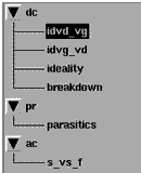
The DUTs and Setups
The DUT/Setup panel is the central access point for the measurement and extraction procedures. The DUTs (for example DC), indicated by the inverted triangles, are groupings of similar measurement setups used to extract related model parameters. The setups contain the information used to define the inputs and outputs for each measurement, as well as their measurement hardware configurations and their associated transforms and plots.
Figure 15 The CGaashf DUT/Setup Panel
|
|
Making the DC Measurements
The DC measurement procedures measure DC current or voltage vs bias under different bias conditions. Setting up the measurement conditions involves two main processes for each measurement setup: defining the instrument state for the DC source/monitor, and setting the input values for the device measurement.
Leave the network analyzer disconnected from the bias networks while you perform the DC measurements, with the RF IN connectors of the bias networks terminated to prevent possible bias oscillation.
Defining the Instrument States
For each of the measurement setups, it is necessary to define the instrument states (options) for the measurement instruments that will be used in that setup. The instrument states need to be defined individually for each setup. Different setups use different measurement instruments. However, with minor exceptions that will be explained, the instrument states for the same measurement type must be used for all the setups that use that measurement type.
| 1 |
After you have selected a setup, for example idvd_vg, the setup window tabs are displayed. |
| 2 |
Select the Instrument Options tab, and a window is displayed showing the instrument states for all instruments used in that measurement. In the DC measurement setups, the instrument states for the DC source/monitor are displayed. In the S-parameter measurement setups, the instrument states for both the DC source/monitor and the network analyzer are displayed. |
The instrument state settings are explained in this chapter with their corresponding setups.
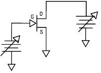
Measuring the Characteristic Curves (idvd_vg)
This procedure measures drain current with respect to drain voltage, at several values of gate voltage. The drain voltage is swept from 0V to the upper limit of its normal operating range.
FET Configuration: The input values you set in the following procedure configure the FET as shown in the following figure.
Figure 16 FET Bias Configuration for idvd_vg Measurement
|
|
Parameters to Be Extracted
This procedure is done first to determine whether or not the device is good. The data from this measurement will be used to extract beta2 and gamma2, the Curtice Cubic parameters that control the linear and saturation regions of device operation. RDS0 (intrinsic output resistance) is also extracted from this measurement through optimization. (In a Curtice quadratic model, this data would be used to extract the beta, gamma, and alpha coefficients.)
This data can also be used for later comparison with predicted data provided by the extracted model.
Defining the DC Source/Monitor Instrument State
Follow the steps described in the appropriate chapter shown next:
Then return to this chapter and continue.
Setting the idvd_vg Input Values
This procedure defines the input signals to be applied to the device under test for this measurement. The actual settings you use will be dependent on the compliance limits for both the device and the SMUs/bias networks, and on the range of measurements you want to take.
If you are measuring a series of devices of the same type and have already set the input values, go directly to the section Measuring and Plotting. Otherwise, select the idvd_vg setup (from the DC DUT) and use the following instructions as a starting point to set up the measurement for your particular device. Refer to your device data sheet as needed for specifications and compliances.
Table 5 For the vd input
|
|
Mode
|
V (voltage)
|
Compliance
|
no greater than the maximum breakdown current value in the device data sheet. With a voltage input, compliance refers to current. Compliance values limit SMU output voltage or current and prevent damage to the device under test, as well as to the SMUs, bias networks, and probes if used.
|
Sweep Type
|
LIN to provide a linear voltage sweep from start to stop voltage values
|
Start
|
0.0
|
Stop
|
Referring to the data sheet for your device, set the Stop value  the upper limit of the device's normal operating range. the upper limit of the device's normal operating range.
|
# of Points
|
Set the # of Points to 21 or less.
|
The Step Size is calculated automatically in software from the start/stop values and number of points. (Alternatively you can set the Step Size and the # of Points is calculated automatically.) Note, however, that the step size must be an integer multiple of the minimum step size of the SMU (refer to the Agilent 4142 Operation Manual for the SMU specifications).
|
Table 6 For the vg input
|
|
Mode
|
V (voltage)
|
Compliance
|
no greater than the maximum allowable gate current value in the data sheet. With a voltage input, compliance refers to current. Compliance values limit SMU output voltage or current and prevent damage to the device under test, as well as to the SMUs, bias networks, and probes if used.
|
Sweep Type
|
LIN to provide a linear voltage sweep from start to stop voltage values
|
Start, Stop, and # of Points
|
Set such that three to five values (points) will be measured, in a range from approximately Vgs=Vpinchoff to Vgs=0V. Set Start to a value close to Vpinchoff, but not so close that the curve will be difficult to discern. (Since the data sheet is likely to provide a range of values, these settings may need to be changed after the first measurement.)
|
|
Caution
|
|
|
|
|
In setting vg, be careful not to set gate voltage values high enough to damage the device.
|
|
| • |
The Outputs are factory set, and should not be changed, with the exception of Type. This is the type of data to be plotted, M for measured, S for simulated, or B for both. There is a tradeoff in making this choice: if the measurement will be a slow one because of long integration time or large number of points, you can save time by setting Type to M. If the measurement will be fast, you can save the need to change the plot Type later during extraction by setting B. Set it to M for now, to save time in plotting the measured values. |
| • |
The Unit names must conform to the names set in the hardware window. Refer to the appropriate chapter as follows: |
- They must also correspond with the actual plug-in SMU connections from the Agilent 4142. Set the vd Unit to VD and the vg Unit to VG. Since the source is grounded, only the drain and gate inputs need to be set.
Measuring and Plotting
This procedure triggers the device measurement, controlling the DC source/monitor to supply the signals you defined in the instrument options and the inputs, and monitors the results.
|
Note
|
|
|
|
|
Remove any high-intensity light sources such as microscope light before taking a measurement. One simple method of blocking light is to place an opaque plastic box on the fixture directly above the device.
|
|
| 1 |
From the idvd_vg setup select the Plots tab. |
| 2 |
Select the id_vs_vd plot, and Display Plot. |
| 3 |
If you have not already connected the DUT, do so now. Observe antistatic precautions. |
| 4 |
Select Measure/Simulate > Measure. Do not touch the fixture or the bias networks while the system is measuring. When the measurement is complete, the yellow MEASURING light on the DC source/monitor goes out, the IC-CAP wristwatch icon goes away, and the measured data is displayed in the plot window. |
| 5 |
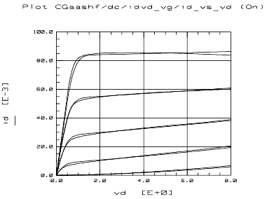
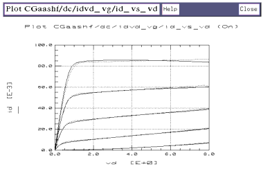
The plotted data should resemble the following figure, with the lowest curve close to the X-axis to show the pinchoff characteristics. If the data indicates the device is not operating in its normal range, you may need to change the gate voltage values you set in the inputs. (If more than one curve is low, change vg Start to a higher value. Or if all the curves are high, change vg Start to a lower value.) Then select Measure again. |
Figure 17 Example idvd_vg Measurement of FET Characteristic Curves
|
|
| 6 |
If the measured data looks wrong for your device, check the probe contacts, the bias connections, and the measuring instruments. Make sure the device is oriented properly, with the right ports connected to the right terminals. If none of these resolves the problem, the device may be defective. For example, if all the curves are superimposed, the gate may be shorted. |
| 7 |
If you wish, you can save the measured data for later comparison with data predicted by the extracted model. To do so, from the Main window, select File > Save As. Use the File Type suffix .set. Enter an appropriate filename (for example dc_test), and press Return or click OK to save the file. |
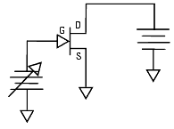
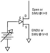
Measuring Drain Current vs Gate Voltage (idvg_vd)
This procedure measures drain current as a function of swept gate voltage, at a single drain voltage bias point in the typical operating range of the device. Values of gate voltage are selected to take the device from pinchoff to IDSS.
FET Configuration: The input values you set in the following procedure configure the FET as shown in the following figure.
Figure 18 FET Bias Configuration for idvg_vd Measurement
|
|
Parameters to Be Extracted
This is a very important measurement, because the A coefficients will be determined from it. The A coefficients form the core of a Curtice cubic model, and therefore must be carefully extracted. Poor measurement and extraction can result in a device model in which the DC performance appears reasonable while the AC performance, specifically S21, is suspect.
Defining the DC Source/Monitor Instrument State
Follow the steps described in the appropriate chapter shown next:
Use the same settings for the idvg_vd setup as you did for the idvd_vg, except set Integ Time to L (long) for maximum averaging, because this measurement uses a derivative process. Note: The instrument states need to be set independently for each setup.
Then return to this chapter and continue.
Setting the idvg_vd Input Values
Select the idvg_vd setup and use these guidelines for setting the vd and vg inputs.
Table 7 For the vd input
|
|
Sweep Type
|
CON (constant) to provide a constant voltage at one bias value
|
Value
|
at or near the typical operating region of the device.
|
Table 8 For the vg input
|
|
Sweep Type
|
LIN (linear)
|
Start and Stop
|
Set such that the gate voltage takes the device from pinchoff to IDSS. It is best to set a start value below 0.0V to avoid contaminating lesser values of drain current with the heat generated at IDSS. The Curtice model does not compensate for heating effects, which would cause a downslope in the measured data at the higher values of drain current.
|
# of Points
|
Set fairly large (>100) to ensure an adequate set of measurements across the voltage range.
|
Measuring and Plotting
| 1 |
From the Plots tab, select the id_vs_vg plot, and Display Plot. |
| 2 |
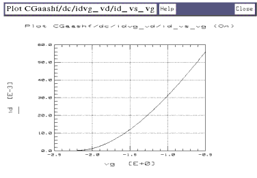
Select Measure/Simulate > Measure. The plot will be updated with the measured data, which should resemble the following illustration. Typically Id increases parabolically with the increase in Vg. If not, there may be a problem with the device. |
Figure 19 Example idvg_vd Measured Data
|
|
| 3 |
Save the data using File > Save As and a filename with the suffix .set. |
Measuring Ideality
This setup forces the FET into a forward-biased diode configuration (gate-source junction), by applying a swept voltage at the gate and opening the drain. Gate-source current is measured as the gate voltage is swept.
FET Configuration: The input values you set in the following ideality procedure configure the FET as shown in the following figure.
Figure 20 FET Bias Configuration for the Ideality Measurement
|
|
Parameters
The data from this DC measurement will be used to extract the diode parameters VBI (built-in voltage), IS (junction saturation current), and N (ideality factor).
Defining the DC Source/Monitor Instrument State
Follow the steps described in the appropriate chapter shown next:
Use the same settings for ideality that you did for the idvg_vd setup, and set Integ Time to L (long).
Then return to this chapter and continue.
Setting the ideality Input Values
|
Caution
|
|
|
|
|
Since the gate-source junction is forward-biased in this configuration, be particularly careful in setting compliance values.
|
|
Select the ideality setup and use these guidelines for setting the vg and id inputs.
Table 9 For the id input
|
|
Mode
|
I
|
Value
|
0.0 to float the drain
|
Sweep Type
|
CON (constant)
|
Compliance
|
In current mode, compliance refers to voltage. If the device data sheet specifies a maximum drain voltage, use that value for Compliance.
|
Table 10 For the vg input
|
|
Compliance
|
a good rule of thumb is to use 0.1 mA gate current per micron of gate width (for example 50 mA for a 500 um device). Allowing too high a current compliance can overstress the device and degrade its performance, even though the results may not be obvious.
|
Sweep Type
|
LIN (linear) for a swept voltage from Start to Stop values
|
Start and Stop
|
Start with conservative values for gate voltage to prevent possible damage to the device. They can quickly be changed after the first measurement if necessary. The FET data sheet is unlikely to specify diode characteristics, so start with best-guess values. Begin by setting a vg Stop value of 500.0m, and increase it if appropriate until the measured data shows the characteristics explained under Measuring and Plotting (The increase must be an integer multiple of the SMU step size.) A typical gate voltage range is from 100 mV to 800 mV.
|
# of points
|
Use a large enough # of points to ensure distribution of measurements across the exponential region of the diode characteristics.
|
Measuring and Plotting
| 1 |
From the Plots tab, select the ig_vs_vg plot, and Display Plot. |
Figure 21 Example Measured ideality Data
|

|
| 2 |
Select Measure/Simulate > Measure. The plotted data should be similar to the illustration. (Note that Ig is plotted on a log scale to show the exponential behavior of the diode junction.) The current should be very low at the low end, and the curve should bend at the high end where the parasitic gate and drain resistances are having an effect. The trace should be smooth and noise-free if a long integration time was used. Noise at the low end occurs if a shorter integration time is used. |
| 3 |
The bend at the high end of the curve defines where the parasitics start dominating, and sets the bounds for extraction. If the displayed data does not show this bend, go back to the inputs and increase the Vg Stop value slightly (perhaps by 100 mV). Repeat the measurement. Iterate as necessary, gradually increasing Vg Stop until the bend in the trace does appear. |
| 4 |
The other plot is used later, in the extraction process. |
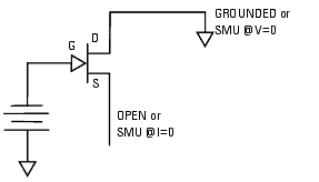
Measuring Breakdown Characteristics (Optional)
Breakdown is not normally a factor in small-signal device operation, typically only occurring if the device is driven hard. The usefulness of this measurement is limited, since the model's extraction of VBR (breakdown voltage) defines a hard breakdown point, while MESFETs typically have a soft breakdown characteristic. However, breakdown is one source of nonlinearity, so you may want to measure and model it. Be aware, however, that it may cause prediction of false harmonic values when the model is used in a simulation.
In this measurement, the source is open and the drain grounded. The gate current is monitored as gate voltage is swept from a positive voltage in the saturation region to a negative voltage beyond the expected reverse breakdown point. If you have a standard system with two SMUs, either disconnect the GNDU SMU from the source and leave it open, or reverse the source and drain connections (GNDU at the drain and SMU2 at the source).
Figure 22 FET Bias Configuration for breakdown Measurement
|
|
Defining the DC Source/Monitor Instrument State
Follow the steps described in the appropriate chapter shown next:
Use the same settings for breakdown as you did for ideality. Integ Time can be set to M (medium).
Then return to this chapter and continue.
Setting the breakdown Input Values
Select the breakdown setup and use these guidelines for setting the vg and vd inputs.
Table 11 For the vg input
|
|
Compliance
|
Set a small value to prevent damage to the device in the reverse breakdown region. 500A is appropriate
|
Sweep Type
|
LIN for a linear voltage sweep from Start to Stop
|
Start
|
a positive value in the saturation region
|
Stop
|
a negative voltage beyond the expected reverse breakdown point
|
Table 12 For the vd input
|
|
Compliance
|
small
|
Sweep Type
|
If you disconnected the source and left it open, set Sweep Type to CON (constant), with a value of 0.0. (Alternatively, connect the GNDU SMU to the drain.)
|
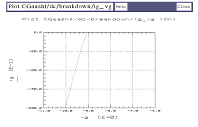
Measuring and Plotting
| 1 |
From the Plots tab, select the ig_vg plot, and Display Plot. |
| 2 |
Select Measure/Simulate > Measure. The measured data should be similar to that shown in the following figure. VBR (breakdown voltage) is the gate voltage Vg value at which gate current Ig stops increasing. |
Figure 23 Example breakdown Measurement Data
|
|
Calibrating the Network Analyzer
It is important to calibrate the network analyzer before you perform the S-parameter measurements. Good calibration of the network analyzer is critical to a good measurement and extraction.
For this procedure, the network analyzer must be calibrated over a broadband frequency range at least equal to the operating range of the device. No subset calibration is required.
For step-by-step calibration procedures, refer to the appropriate chapter as follows:
Then return to this chapter and continue.
|
Note
|
|
|
|
|
IC-CAP requires values to be entered into the software regarding calibrations, instrument states, and measurement values. It is important that values entered in software correspond with actual instrument settings.
|
|
Making the S-Parameter Measurements
The swept S-parameter measurements in the next two setups provide the data that allows extraction of parameters related specifically to the high-frequency performance of the device. A swept-frequency signal is applied to the gate, and the device S-parameters are measured at the drain.
Setting up the measurement conditions involves processes similar to those for the DC measurements: defining the instrument states and setting the input values for each measurement.
Measuring S-Parameters vs Frequency
This procedure measures S-parameters across a calibrated microwave frequency range, with a fixed bias value in the typical linear operating region of the device.
FET Configuration: The input values you set in the following s_vs_f procedure configure the FET as shown in the following figure.
Figure 24 FET Bias Configuration for the s_vs_f Measurement
|
|
Parameters
The data from this measurement will be used to extract RIN, RDG, CDGN, RDGN, CDG, CGS0, A5, and RC.
Defining the Instrument States
Follow the steps described in the appropriate chapter shown next:
Set the Cal Set No to the cal set or register where you stored the broadband calibration you performed earlier. The procedures in this manual use cal set #1.
Then return to this chapter and continue.
Setting the s_vs_f Input Values
Connect the network analyzer RF input cables to the RF IN ports of the bias networks and select the s_vs_f setup.
Table 13 For the freq input
|
|
Mode
|
F
|
Sweep Type
|
LIN (linear) for a linear measurement sweep across the frequency range.
|
Sweep Order
|
1
|
Start, Stop
|
Set the Start and Stop values to correspond with the frequency you defined in your broadband calibration.
|
# of Points
|
The same as in the calibration.
|
Table 14 For the vd input
|
|
Mode
|
F
|
Sweep Type
|
CON (constant), to provide fixed bias values of both gate and drain voltage
|
Compliance
|
no greater than the maximum breakdown current value in the device data sheet
|
Value
|
bias the device in a typical linear operating region of the device
|
Table 15 For the vg input
|
|
Compliance
|
no greater than the maximum allowable gate current value
|
Sweep Type
|
CON (constant), to provide fixed bias values of both gate and drain voltage
|
Value
|
bias the device in a typical linear operating region of the device
|
| • |
The Outputs are factory set, and should not be changed, except for Type. To reduce time in plotting all four S-parameters, you can set Type to M (medium) for now. |
Measuring and Plotting
| 1 |
Select Plots > Display All. This displays all the plots at the same time. Alternatively, you can display them one-by-one using the method explained in the other measurement procedures. |
| 2 |
Select Measure/Simulate > Measure. The plotted data should be typical for your device. The illustrations below show measured S-parameter data for an example device. If the results are unexpected, recheck the values you set in the inputs and instrument options. In particular, be sure the instrument states and input stimulus signals match the values set in the network analyzer calibration. |
| 3 |
If you change the inputs or instrument states, repeat the measurement. If the data still looks abnormal, the device may be defective. |
| 4 |
Save the measured data using File > Save As and a filename with the suffix .set. |
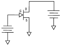
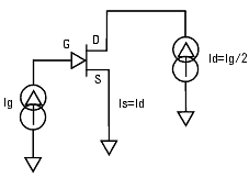
Measuring Parasitic Resistances and Inductances
This procedure uses S-parameter measurements to determine the device parasitic resistance and inductance values. It measures S-parameters vs frequency, with both the gate-source and gate-drain junctions strongly forward biased, and fixed values of gate and drain current. Drain current is set to one half gate current, to force Is = Id: this makes the intrinsic Vds zero, removing the channel resistance. The device can thus be modeled as a T-network.
FET Configuration: The input values you set in the following parasitics procedure configure the FET as shown in the following figure.
Figure 25 FET Bias Configuration for parasitics Measurement
|
|
This measurement is done last because of the high gate current applied to the device. However, this high current should not be a problem because the power dissipation is not correspondingly high with Vds forced to zero. Theoretically, if the parasitic resistance were large enough for heat to be generated, the device could be damaged, but this situation is highly unlikely.
Parameters
The data from this measurement will be used to extract all the parasitic resistance and inductance values: RG, RD, RS, LG, LD, and LS.
Defining the Instrument States
Follow the same procedure you used in the s_vs_f measurement. Use the same settings.
Setting the parasitics Input Values
| 1 |
Select the parasitics setup. |
| 2 |
Set the input values under freq the same as for the s_vs_f measurement, as you will be using the same network analyzer calibration. |
| 3 |
Set the id Compliance as high as the device maximum Vds value or higher. The voltage compliance should not be so low as to inhibit current flow in this measurement. |
| 4 |
Set the ig Compliance as high as the device maximum Vgs value or higher. |
| 5 |
Set the Sweep Type to CONstant for both id and ig to provide fixed current values. |
| 6 |
Set the id current Value to ID and the ig Value to IG. Numerical values are assigned to these variables as follows: |
| |
• |
To ensure that the Is = Id = Ig/2 relationship is maintained, the ratio between gate current and drain current is defined in the setup variable table. This allows the gate current to be set to a numerical value and the drain current to be specified with respect to the gate current. |
| |
• |
Select the Setup Variables tab. A variable table is displayed where you can define Ig and Id. |
| |
• |
Set the IG current value based on gate width: 0.1 to 0.2 mA per micron. Thus for a device with 500 um gate width, Ig would be 100 mA. This may seem like a lot of gate current, but the larger Ig is, the smaller the dynamic impedance becomes. |
| |
• |
Set the ID current to -IG/2, to force Is = Id. |
Measuring and Plotting
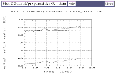
| 1 |
From the Plots tab, select the R_data plot, and Display Plot. |
| 2 |
Select Measure/Simulate > Measure. |
| 3 |
To make sure the SMUs did not compliance-limit during this measurement, check the UNIX window for an error message to that effect. If the SMUs did reach compliance limit, the current may not have been balanced in the drain and source, which will cause misleading extraction results. In this case, go back to the inputs and increase the ig and id Compliance values by as much as 10 to 20%. |
| 4 |
The measured data should resemble the following illustration. The annotation shows the resistance data as the real part of the device impedance Z. The displayed traces are the measured values for Rs, Rd, and Rg. |
Figure 26 Example Parasitic Resistances
|
|
| 5 |
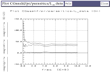
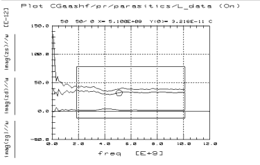
Select the L_data plot, and Display Plot. The plotted data should resemble the illustration. The annotation shows the inductance data as the imaginary part of the device impedance Z. The displayed traces are the measured values for Ld, Lg, and Ls. |
Figure 27 Example Parasitic Inductances
|
|
| 6 |
Leave the parasitics setup open, as it is the first setup used in the extraction process. |
Parameter Extraction
Now that all the measurements have been made, the extraction process can begin. There is no single clear and exact procedure for extracting parameters: the process is very iterative and subjective. The goal is to create a list of device parameters that can be used in a model to accurately predict performance. A key to success is that the parameters must be realistic. Because of the inherent coupling of the model equations, a variety of parameter value combinations will result in a good match between simulated and measured data.
The specific measurement setups are defined for the purpose of decoupling the model equations as much as possible. In this way, the effects of individual parameters or small groups of related parameters can be isolated, and their values determined with reasonable certainty. However, no matter how good the measurement setup, there is always some interaction between parameters. Therefore, during the extraction process, the validity of the extracted parameters must be constantly scrutinized.
The ability to discern reasonable values from questionable ones comes from knowledge of device physics, knowledge of the particular device, and individual experience. Parameter extraction is still very much an art.
Parasitic Extraction
In all the equations governing the behavior of the model, the voltages are assumed to be intrinsic. There is no direct way to measure or set the intrinsic voltages, so they must be determined indirectly. To accomplish this, the parasitic resistances and inductances must first be very accurately determined. Once these are known, the intrinsic voltages can be calculated from these parasitic values and the known currents, using the following equations:
DC:
- VGSint = VGSext - Ig · RG - Is · RS
- VDSint = VDSext - Id · RD - Is · RS
AC:
- vgsint = vgsext - ig(RG + j
 LG) - is(RS + jLS) LG) - is(RS + jLS)
- vdsint = vdsext - id(RD + jLD) - is(RS + jLS)
These intrinsic voltages are used by the Curtice cubic model to predict device performance, so they must be known before any other parameters can be extracted.
Selecting the Simulator
One last step remains before the actual extractions: to check that the selected simulator is compatible with the model. The only simulator that supports the Curtice GaAs model is hpspice.
- Select the Model Variables tab. A variable table is displayed, showing the name of the currently selected simulator. If the SIMULATOR name is not hpspice, then type hpspice.
Displaying the Parameters Table
The CGaashf Model Parameters table lists all the parameters that will be extracted, and initially displays default values. As you perform the individual extractions, the default values change to extracted values. Throughout the extraction process, you will use the Parameters table to read extracted values, and to enter or modify values to adjust interactive parameters for best agreement of simulated with measured data. In addition, you can set limits by entering minimum and maximum values for each parameter. Parameter values that are outside their limits are clamped to their minimum or maximum values. To view the parameters, click the Model Parameters tab.
Extracting Parasitic Resistances and Inductances
This procedure extracts the parasitic gate, drain, and source resistances (RG, RD, RS) and gate, drain, and source inductances (LG, LD, LS). These parameters are extracted from the S-parameter data measured with the parasitics setup.
| 1 |
Locate the default values for RG, RD, RS, LG, LD, and LS in the Parameters table. |
| 2 |
Select the parasitics setup from the DUT/Setup panel. |
| 3 |
From the Plots tab, select R_data > Display Plot, and L_data > Display Plot. |
| 4 |
From the Extract/Optimize tab, select the autoextract transform and Execute. The transform calculates the parasitic values with frequency and enters them in the Parameters table. In the plots, the resistance data displayed is the real part of the device impedance Z, and the inductance data is the imaginary part of the impedance. |
| 5 |
Select the zg transform and Execute. The transform data is added to the R_data and L_data plots. |
| 6 |
To verify the RG and LG data values in the Parameters table against the values plotted, position the pointer at a frequency of interest or on some approximately median point on the trace, and click middle. A readout of the trace value (Y) at that point is listed above the plot: compare this value with the value in the Parameters table. |
| 7 |
If the trace value you selected and the Parameters table value do not closely correspond, it may be because a portion of the trace is noisy. In particular, the inductance values at the lower frequencies are likely to be noisy and less valid. You may wish to change the Parameters table value to more closely represent a linear portion of the trace. The parasitic values calculated by autoextract are averaged across the entire frequency range of the measurement by default. To average across only a portion of the trace you can use the X-low/X-high function. |
| |
• |
Select the Setup Variables tab. A variable table will appear, listing X_LOW and X_HIGH with their default or current frequency values. |
| |
• |
From the plotted data choose a linear portion of the trace. Put the mouse pointer at the low end of that portion and click left, then put the pointer at the high end and click left to make a box on the trace, as shown in the illustration. |
Figure 28 Selecting a Linear Portion of the L_data Trace
|
|
| |
• |
From the plot menu select Options > Copy to Variables. This changes the X_LOW and X_HIGH values in the table to the values you selected on the trace. |
| |
• |
Repeat autoextract > Execute. The transform recalculates the parasitic values using the new X-low/X-high values. |
| 8 |
Select Extract/Optimize > zd > Execute. To verify the drain resistance and inductance values (RD and LD) in the Parameters table, follow the same steps as for the gate parasitics. |
| 9 |
Select zs > Execute. To verify the source resistance and inductance values (RS and LS) in the Parameters table, follow the same steps as for the gate parasitics. |
Extracting the Gate Diode Parameters
This procedure extracts the parameters N (ideality factor), VBI (built-in voltage), and IS (junction saturation current). These parameters are extracted from the DC data measured with the ideality setup.
N (Ideality Factor)
| 1 |
Scroll the Parameters table until it shows the value for ideality, represented as NMF1.N. |
|
Note
|
|
|
|
|
Several of the parameter names in the table are preceded by NMF1.
|
|
| 2 |
Select DUTs/Setups > ideality. |
| 3 |
Select Plots > n_vs_vg > Display Plot. |
| 4 |
Select Extract/Optimize > extract > Execute. |
| 5 |
Select the n transform, and Execute. This calculates the ideality factor and enters it into the Parameters table. |
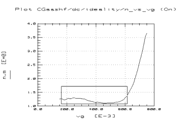
| 6 |
The data displayed in the n_vs_vg plot should resemble Figure 29. N is computed as the minimum value along the linear region of the logarithmic curve (shown in the box in Figure 29). Beyond the linear region, the parasitic values begin to dominate, and N is no longer identifiable. |
| 7 |
To check the N value in the Parameters table against a value on the trace, put the mouse pointer on the linear portion of the trace and click middle for a readout of the Y-axis value at that point. |
| 8 |
If the n_vs_vg plot looks significantly different from the following figure, the N value in the Parameters table may not be valid. For example, if noise is present on the trace below the linear region of the curve, N may have been computed as the minimum value of the noise. In this case, use the X-low/X-high function to get a more valid value. |
Figure 29 Linear Portion of the n_vs_vg Plot
|
|
| 9 |
To compute N over only the linear portion of the trace using X-high/X-low: |
| |
• |
Select Setup Variables to open the X-high/X-low variable table. |
| |
• |
In the Value field (right side of the table) for OVERRIDE_LIMITS, change FALSE to TRUE, to set override limits to true. |
| |
• |
Make a box on the trace by clicking left on the ends of the linear portion. |
| |
• |
From the plot menu select Options > Copy to Variables to change the X-low/X-high values to the trace limits you selected. |
| |
• |
Select Extract/Optimize > extract > Execute to recalculate the N value using the new X-low/X-high values. |
| |
• |
Check the value of NMF1.N in the Parameters table. |
| 10 |
If no linear region is shown on the trace, a valid ideality factor cannot be computed from it. In this case, you will need to manually enter a value of 1 or 0. Since the contribution of N to the gate current is relatively small, it is best when the data is very nonlinear to eliminate the contribution of the N factor by using a value of 0. To change the NMF1.N value in the Parameters table, move the mouse pointer over the current entry and click left to highlight it, then type in the new value and press Return. |
IS (Saturation Current)
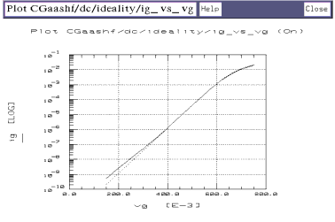
| 1 |
Select Plots > ig_vs_vg > Display Plot. The data displayed should resemble the following figure, with two plotted functions of gate current Ig vs gate voltage Vg. The solid line is the measured data, and the dashed line is the simulation. |
Figure 30 Measured and Simulated Saturation Current (IS) Data
|
|
| 2 |
Scroll the Parameters table until it shows the value for NMF1.RF. |
| 3 |
Select DUTs/Setups > Extract/Optimize > rf_off > Execute. The value of NMF1.RF in the Parameters table will change to 0. |
| 4 |
Scroll the Parameters table until it shows the value for NMF1.IS. |
| 5 |
Select Extract/Optimize > opt_is > Execute. Observe the plot and see the simulated data converge on the measured data as the value for IS is optimized. (Note that the opt_is transform optimizes the linear data for which the ideality factor is valid.) |
| 6 |
Observe the change in the Parameters table value for IS. |
| 7 |
The parameter value for VBI is also changed. |
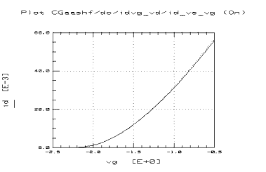
Extracting the A Parameters and VDS0
This procedure extracts and optimizes the A0, A1, A2, and A3 coefficients that describe the threshold characteristics of the device. VDS0 is the value of VDS at which A0 through A3 are determined; its default value is the value of Vd specified in the idvg_vd inputs.
These parameters are extracted from the DC data measured with the idvg_vd setup.
| 1 |
Scroll the Parameters table until it shows the default values for A0, A1, A2, and A3. |
| 2 |
Select DUTs/Setups > idvg_vd. |
| 3 |
Select Plots > id_vs_vg > Display Plot. |
Figure 31 A Parameter Data After Optimization
|
|
| 4 |
Select Extract/Optimize > extract > Execute. |
| 5 |
The transform calculates the values of A0, A1, A2, A3, and VDS0 and enters them into the Parameters table. |
| 6 |
Scroll the Parameters table until you find the value for NMF1.VDS0. Manually enter this same value into the Parameters table for VDSDC (you will need to scroll the Parameters table again to find it). |
| 7 |
Select Measure/Simulate > Simulate. The plot should now display a solid-line measured curve and a dashed-line simulated curve. |
| 8 |
Select Extract/Optimize > opt_cubic > Execute. Watch the simulated data converge on the measured data as the values for the A coefficients are optimized (as in Figure 31). |
| 9 |
Select Model Parameters, and observe the new Parameters table values for the A coefficients and VDS0. |
Extracting Beta and Gamma Parameters and RDS0
This procedure extracts beta2 and gamma2, the Curtice cubic parameters that control the linear and saturation regions of device operation. Gamma2 dominates in the linear region and determines the transition from linear to saturation; beta2 dominates in the saturation region.
Also extracted through optimization is RDS0, the intrinsic output resistance. RDS0 dominates at both the low and high values of Vds relative to VDS0 (that is, Vds VDS0 and VDS0 Vds).
These parameters are extracted from the DC data measured with the idvd_vg setup.
| 1 |
Scroll the Parameters table until you find RDS0. Manually set an RDS0 value of 1K ohms, as the initial value to be used in the optimization. |
| 2 |
Select the idvd_vg setup. |
| 3 |
Select Plots > id_vs_vd > Display Plot. |
| 4 |
Select Extract/Optimize > extract > Execute. |
| 5 |
Select Measure/Simulate > Simulate. |
| 6 |
The plot should now display a family of solid-line measured curves and dashed-line simulated curves, as in the following figure. |
Figure 32 Measured and Simulated Data for Beta, Gamma, and RDS0 Extraction
|
|
| 7 |
Select Extract/Optimize > opt_cubic > Execute. Watch the simulated curves converge on the measured curves as the beta and gamma coefficients are optimized. |
| 8 |
Scroll the Parameters table and observe the new values for BETA, GAMMA, and RDS0. |
Extracting the AC and Capacitance Parameters
This extracts the parameters RIN, RGDN, CGDN, CDS, CGS0, A5, and RC. These parameters are extracted from the S-parameter data measured with the s_vs_f setup. The transforms calculate the intrinsic admittances vs frequency.
In an extraction of admittances vs frequency, the linear region of the data may be bounded by nonlinearities at the ends of the frequency range. Capacitance tends to dominate at lower frequencies, and inductance at higher frequencies. The most appropriate values for the extracted parameters occur in the linear resistive region of the data. The X-low/X-high function lets you define the boundaries of the linear region and perform the transform over only that region.
| 1 |
Select the s_vs_f setup. |
| 2 |
Select the Plots tab, then select and display the following plots: Rs, Cs, tau_a5, and CGS0. |
| 3 |
Select the Extract/Optimize tab, then select and execute the following transforms: ygs, ygd, yds, a5, cgs0, and ygm. |
| 4 |
Examine the plots and use the X-low/X-high function if necessary to limit the range of the extractions that will follow: |
| |
• |
Select Setup Variables to open the X-high/X-low variable table. |
| |
• |
Click left at the ends of the linear region to make a box on the trace. |
| |
• |
From the plot menu select Options > Copy to Variables to change the X-low/X-high values to the trace limits you selected. |
| |
• |
Select Extract/Optimize > extract > Execute to recalculate the parameter values using the new X-low/X-high values. |
| 5 |
Select extract_RC > Execute. This transform optimizes RC to minimize the difference between the measured real yds and the simulated real yds. |
| 6 |
Verify the values of the extracted parameters listed in the Parameters table against the measured data in the plots. |
| |
• |
The Cs plot shows the value for CGDN as imag(ygd), the imaginary part of the measured gate admittance; and CDS as imag(yds), the imaginary part of the measured drain admittance. |
| |
• |
The Rs plot shows RIN as real(ygs), the real part of the measured gate admittance; and RGDN as real(ygd), the real part of the measured drain admittance. |
| |
• |
The CGS0 plot shows CGS0 as real(cgs0). |
| |
• |
The tau_a5 plot shows A5 as imag(a5). |
Verifying the AC and Capacitance Extractions
| 1 |
Select Plots > S11 > Display Plot. Repeat this for S12, S21, and S22. |
| 2 |
The plots show the measured and simulated S-parameter values. If the extraction is good, the simulated traces should converge toward the measured traces, as in the S-parameter plots below. |
| 3 |
If the simulated traces do not match the measured traces well, recheck the extracted R, C, and L values. |
This ends the extraction process.
Storing the Model
This procedure stores the model in IC-CAP, including all the device-specific measured and simulated data. Once you have developed the device model, it can be used as a component in the Agilent RF and Microwave Design System (MDS). You can use it for circuit simulation, inserting it into circuits under design to emulate the characteristics of your device.
If you will be modeling large numbers of devices, it is worthwhile to organize your directory structure according to device type, geometry, and batch or wafer.
| 1 |
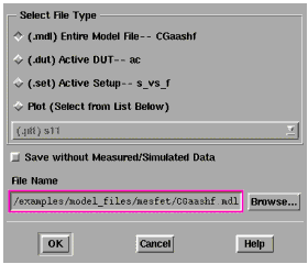
Use the UNIX directory you created at the beginning of the procedure, when you first opened the CGaashf.mdl file. |
| 2 |
From the CGaashf:1 main menu select File > Save As. |
| 3 |
A dialog box is displayed, as illustrated. |
Figure 33 Save As Dialog Box
|
|
| 4 |
Select the File Type (.mdl for a complete model) by clicking the corresponding radio button. |
| 5 |
Select a new filename that associates this model with the device, for example fet5.mdl. Type the full directory pathname and the filename into the dialog box. Select OK to store the data and close the dialog box. |
Storing the Parameters Table
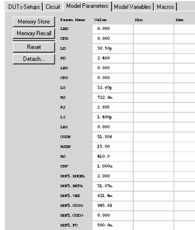
The Parameters table lists all the parameters extracted for a device model. You can save the Parameters table for a specific device. The illustration shows a portion of the table.
Figure 34 Top Portion of the Model Parameters Table
|
|
| 1 |
To save the Parameters table select File > Save As. |
| 2 |
In the dialog box, select the File Type .mps for model parameter set. |
| 3 |
Type in a filename or use the one in the File Name field. |
You can now recall the same set of device parameters any time you wish.
|