Using the High-Frequency BJT Model
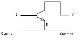
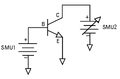
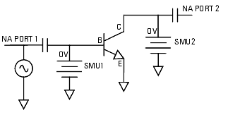
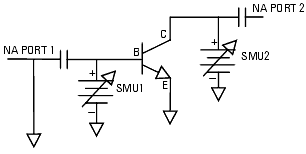
To effectively isolate the individual parameters of a BJT, some device measurements require that the collector is biased and the emitter grounded, while some require that the emitter is biased and the collector grounded. These procedures assume that in-fixture measurements are made with the device mounted in the fixture in a common-emitter configuration as shown in the following figure. In some measurements, the collector is synchronized to the emitter with an offset, to provide data equivalent to that of a common-collector configuration.
Figure 35 BJT in Common-Emitter Configuration
|
|
|
Note
|
|
|
|
|
An earlier version of the Agilent 85193A high-frequency BJT model made use of a BJT switching adapter to switch the device between biased-collector and biased-emitter configurations. Now a synchronized sweep (SYNC) is used to synchronize the base and collector SMUs together, allowing all measurements to be made using a common-emitter configuration thus eliminating the need for the switching adapter. The earlier model, bjt_nhf, can still be used, along with the switching adapter, if you prefer.
|
|
The procedures in this chapter include detailed instructions for:
| • |
Setting the instrument states for each measurement |
| • |
Setting the input values for each measurement |
| • |
Making the measurements and qualifying the results |
| • |
Extracting DC, capacitance, and AC parameters; optimizing the results |
| • |
Verifying the simulated performance against measured data |
| • |
Adjusting the extracted parameters for best model accuracy |
|
Note
|
|
|
|
|
Measurement parameters and measured data are specific to individual devices. Information and data are provided here as examples and guidelines, and are not intended to represent the only correct method or results.
|
|
The procedures start with example values for IC-CAP measurement inputs. They provide guidelines on setting the values to measure your device. However, the values you use will be based on your knowledge of your device and on information provided in its device data sheet, as well as on the guidelines provided here: they may or may not correspond with the examples. In some cases, it may be necessary to set the input values, make a measurement, and then reset the inputs based on the measurement results. The procedures give suggestions on judging the applicability of the input values and measured data.
The illustrations of plotted data are provided as visual examples of possible measurement results. They are not intended to represent a sequential measurement of one device, nor do they necessarily correspond with the example measurement inputs described in the procedures. The plots can be used to check the reasonableness of your own measured data, which should appear similar in shape but not necessarily coincident in values.
In addition, the IC-CAP software itself includes measured data for some of the setups. This data is from the measurement of a single device, and shows another example of possible results. Many, though not all, of the input settings for this measurement correspond with the example settings.
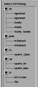
The DUTs and Setups
The DUT/Setup panel is the central access point for the measurement and extraction procedures. The DUTs (for example DC) indicated by the inverted triangles, are groupings of similar measurement setups used to extract related model parameters. The setups contain the information used to define the inputs and outputs for each measurement, as well as their measurement hardware configurations and their associated transforms and plots.
Figure 36 The DUT/Setup Panel
|
|
Making the DC Measurements
The DC measurement procedures measure DC current or voltage versus bias under different bias conditions. Setting up the measurement involves two main processes for each measurement setup: defining the instrument state for the DC source/monitor, and setting the inputs for the device measurement.
Leave the network analyzer disconnected from the bias networks while you perform the DC measurements, with the RF IN connectors of the bias networks terminated to prevent possible bias oscillation.
Defining the Instrument States
For each of the measurement setups, it is necessary to define the instrument states (options) for the measurement instruments that will be used in that setup. The instrument states need to be defined individually for each setup. Different setups use different measurement instruments. However, with minor exceptions that will be explained, the instrument states for the same measurement type must be used for all the setups that use that measurement type.
To define the instrument state for any given setup:
| 1 |
Select the setup, for example fgummel. |
| 2 |
Click the Instrument Options tab, and the window changes to display the instrument states for all instruments used in that measurement. In the DC measurement setups, the instrument states for the DC source/monitor are displayed. In the S-parameter measurement setups, the instrument states for both the DC source/monitor and the network analyzer are displayed. |
The instrument state settings will be explained in this chapter with their corresponding setups.
Making the Forward Gummel Measurement
The forward and reverse gummel measurements plot the operating range of the base and collector currents with the transistor in the forward active and reverse active modes. All coefficients of the DC model equations are derived from the fgummel and the rgummel data.
This procedure measures Ic and Ib with respect to Vbe. The base and collector are swept across a range large enough that both high-level and low-level effects occur. This measurement should always be done first because its result is used to properly define the ranges of subsequent measurement setups.
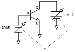
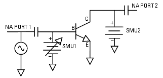
BJT Configuration: The input values you set in the following fgummel procedure configure the BJT as shown in the following figure.
Figure 37 BJT Configuration for fgummel Measurement
|
|
Parameters
The data from this measurement will be used to extract IS, BF, NF, ISE, NE, and IKF. It may also need to be used to interactively modify other parameters such as RE, RC, RB, and VAR.
Defining the DC Source/Monitor Instrument State
Follow the steps described in the appropriate chapter shown next:
However, for the forward gummel measurement, set Integ Time to L (long) to reduce noise at low current values. Then return to this chapter and continue.
Setting the fgummel Input Values
This procedure defines the input signals to be applied to the device under test for this measurement. The actual settings you use will depend on the compliance limits for both the device and the SMUs/bias networks, and on the range of measurements you wish to take.
You provide compliance values to limit SMU output voltage or current and prevent damage to the device under test, as well as to the SMUs, bias networks, and probes, if used. With a voltage input, compliance refers to current. Refer to your device data sheet as needed for specifications and compliances. From the DC DUT select the fgummel setup. The setup inputs and outputs are displayed.
Table 16 For the vb input
|
|
Mode
|
V (voltage)
|
Unit
|
SMU1
|
Compliance
|
no greater than the maximum allowable base current value in the device data sheet.
|
Sweep Type
|
LIN, to provide a linear Vbe sweep from start to stop voltage values
|
Start and Stop
|
Voltage values that define the operating range of the device. The Start value should be low enough so that the Ib curve bends up at the low end due to recombination in the base-emitter depletion region. The Stop value should be large enough so that the Ic curve begins to bend over at the high end due to high-level effects.
|
# of Points
|
A value sufficiently large such that the subtle bends at the low and high ends of the curves are clearly displayed—51 points is usually an adequate number
|
Table 17 For the ve input
|
|
Mode
|
V (voltage)
|
Unit
|
GND
|
Sweep Type
|
CON
|
Value
|
0.000 to provide a constant zero voltage. This holds the emitter at ground potential to prevent reverse leakage from influencing Ib.
|
Table 18 For the vc input
|
|
Mode
|
V (voltage)
|
Unit
|
SMU2
|
Compliance
|
no greater than the maximum collector current value in the data sheet.
|
Sweep Type
|
SYNC, to synchronize it to the Master Sweep vb.
|
Ratio
|
1.000
|
Offset
|
0.000
|
| • |
The Unit names must conform to the names set in the hardware window. Refer to the appropriate chapter as follows: |
- They must also correspond with the actual plug-in SMU connections from the Agilent 4142.
| • |
The Outputs are factory set, and should not be changed, with the exception of Type. This is the type of data to be plotted, M for measured, S for simulated, or B for both. The illustrations of measured data in this chapter were plotted with the outputs set to M: in the extraction section later in the chapter, where the illustrations show both measured and simulated data, the outputs were set to the default, B. |
Measuring and Plotting
This procedure triggers the device measurement, controlling the DC source/monitor to supply the signals you defined in the instrument options and the inputs, and monitors the results.
|
Note
|
|
|
|
|
Remove any high-intensity light sources such as microscope light before taking a measurement. This is particularly important if currents in the nanoamp range are being measured. One simple method of blocking light is to place an opaque plastic box on the fixture directly above the device.
|
|
| 1 |
From the Plots tab, select the ibicvsvb plot, and Display Plot. |
| 2 |
If you have not already connected the DUT, do so now. Observe antistatic precautions. |
| 3 |
Select Measure/Simulate > Measure. Do not touch the fixture or the bias networks while the system is measuring. The yellow MEASURING light on the DC source/monitor will go off when the measurement is complete. |
| 4 |
The plot will be updated with the measured data. If the Ic curve does not bend over at the high end, go back to the inputs and set vb Stop to a larger value. Be careful, however, not to exceed the maximum current rating of the device. If the Ib curve does not bend up at the low end, set vb Start to a smaller value. Repeat the measurement. |
- The other plots are used later, in the extraction process.
| 5 |
Save the data using File > Save As and a filename with the suffix .set. |
Making the Reverse Gummel Measurement
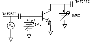
This procedure measures Ie and Ib with respect to -Vce. The emitter and base are grounded, and the base-collector voltage is swept across a negative range wide enough to show both high-level effects and low-level depletion effects.
BJT Configuration: The input values you set in the following rgummel procedure configure the BJT as shown in the following figure.
Figure 38 BJT Configuration for rgummel Measurement
|
|
Parameters
The data from this measurement will be used to extract BR, ISC, NR, IKR, and NC. It may also need to be used to interactively modify other parameters such as RE, RC, RB, and VAF.
Defining the DC Source/Monitor Instrument State
Follow the steps described in the appropriate chapter shown next:
Use the same settings for the rgummel setup as you did for the fgummel.
|
Note
|
|
|
|
|
The instrument states need to be set independently for each setup.
|
|
Then return to this chapter and continue.
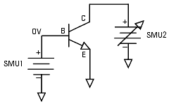
Setting the rgummel Input Values
| 1 |
In the DC DUT select the rgummel setup. |
| 2 |
The vb Value is usually set to 0.000 to prevent reverse leakage from influencing Ib at low -Vc values. |
| 3 |
Set the vc Start value low enough that the Ib curve preferably bends up at the low end due to recombination in the base-collector depletion region. The Stop value should be large enough that the Ie curve begins to bend over at the high end due to high-level effects. Synchronization is not necessary for this measurement. |
| 4 |
Do not change the ve values, which set the emitter to ground. |
Measuring and Plotting
| 1 |
From the Plots tab, select the ibievsvc plot, and Display Plot. |
| 2 |
Select Measure/Simulate > Measure. The plot will be updated with the measured data. If the Ie curve does not bend over at the high end, go back to the inputs and set vc Stop to a larger value. Be careful, however, not to exceed the maximum current rating of the device. Repeat the measurement. |
| 3 |
Save the data using File > Save As and a filename with the suffix .set. |
Making the Forward Early Measurement
The forward early measurement models the effect of base-width modulation due to variations in the base-collector depletion region.
This procedure measures Ic with respect to Vce at a single value of Vbe. The emitter is grounded and the collector voltage is swept. The Vbe value is taken from the log-linear region of the fgummel measurement.
BJT Configuration: The input values you set in the following fearly procedure configure the BJT as shown in the following figure.
Figure 39 BJT Configuration for fearly Measurement
|
|
Parameters
The data from this measurement will be used to extract VAF, the forward early voltage.
Defining the DC Source/Monitor Instrument State
Follow the steps described in the appropriate chapter shown next:
Use the same settings as for the fgummel measurement, except set Integ Time to M (medium) if you prefer. Then return to this chapter and continue.
Setting the fearly Input Values
| 1 |
Select the fearly setup. |
| 2 |
Set Vb to measure at a single constant value. This should be in the log-linear range of the fgummel measurement, between the high- and low-level effects. To determine the Vb value, refer to the measured data from the fgummel measurement. |
| 3 |
The reason for measuring at only one value of Vbe is that the rearly measurement must use the same number of base voltage values. The rearly measurement uses the sync function, and it can only synchronize on one base value. |
| 4 |
Set the vc range with a Start value of 0.0. Referring to the data sheet for your device, set the Stop value  the upper limit of the device's normal operating range. the upper limit of the device's normal operating range. |
| 5 |
Set the vc # of Points sufficient that the resulting Ic curves will be clearly separated and easily distinguishable. |
| 6 |
Do not change the ve values, which set the emitter to ground. |
Measuring and Plotting
| 1 |
From the Plots tab, select the icvsvc plot, and Display Plot. |
| 2 |
Select Measure/Simulate > Measure. The plot will be updated with the measured data. If you are not satisfied with the data, go back to the inputs and change the vb or vc values, staying within the log-linear range of the fgummel measurement for vb. Repeat the measurement. |
| 3 |
Save the data using File > Save As and a filename with the suffix .set. |
Making the Reverse Early Measurement
The reverse early measurement models the effect of base-width modulation due to variations in the base-emitter depletion region.
This procedure measures Ie with respect to -Vce. The base is synchronized to the collector. The Vbc values are taken from the -Vc values in the log-linear region of the rgummel measurement, taking the device from near cutoff to near saturation.
BJT Configuration: The input values you set in the following rearly procedure configure the BJT as shown in the following figure.
Figure 40 BJT Configuration for rearly Measurement
|
|
Parameters
The data from this measurement will be used to extract VAR, the reverse early voltage.
Defining the DC Source/Monitor Instrument State
Follow the same procedure you used in the fearly measurement. Use the same settings.
Setting the rearly Input Values
| 1 |
Select the rearly setup. |
| 2 |
Set the vc range with a Start value of 0 and a Stop value in the negative range. This should be in the log-linear range of the rgummel measurement, between the high- and low-level effects. |
| 3 |
Because vb is synchronized to the master sweep vc, only one vb value can be set. In this example, vb is offset from vc by 670 mV, so that Vb = Vc + 670 mV. The ratio of vb to vc is 1:1. |
Measuring and Plotting
| 1 |
From the Plots tab, select the ievsvc plot, and Display Plot. |
| 2 |
Select Measure/Simulate > Measure. If you are not satisfied with the measured data, go back to the inputs and change the vc values or the vb offset. Repeat the measurement. |
| 3 |
Save the data using File > Save As and a filename with the suffix .set. |
Making the fearly_family Measurement
This setup measures Ic with respect to Vce at three values of Vbe. The collector is set to the same values as in the fearly measurement, but the base voltage is set for measurements at three values. This allows you to view the device behavior over a wider range of base input voltages.
BJT Configuration: The input values you set in the following fearly_family procedure configure the BJT as shown in the following figure.
Figure 41 BJT Configuration for fearly_family Measurement
|
|
Defining the DC Source/Monitor Instrument State
Follow the same procedure you used in the fearly measurement. Use the same settings.
Setting the fearly_family Input Values
| 1 |
Select the fearly_family setup. |
| 2 |
Set the vb # of Points to 3 to allow for measurements at three different values so that you can see the device behavior at different base voltages. One of the base voltage values is the same as the value used in the fearly measurement. |
| 3 |
To determine the Vb values, refer to the measured data from the fgummel measurement. Set vb Start and Stop to values in the log-linear range of the fgummel measurement, between the high- and low-level effects. The step size should be sufficient that the resulting measured Ic curves will be clearly separated and easily distinguishable. |
| 4 |
Set the vc range with Start and Stop values the same as for the fearly measurement. |
Measuring and Plotting
| 1 |
From the Plots tab, select the icvsvc plot, and Display Plot. |
| 2 |
Select Measure/Simulate > Measure. If you are not satisfied with the spacing of the Ic traces, go back to the inputs and change the vb Start and/or Stop values, staying within the log-linear range of the fgummel data. Repeat the measurement. |
| 3 |
Save the data using File > Save As and a filename with the suffix .set. |
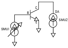
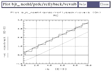
Making the rcflyback Measurement
This procedure drives the base with a current to negate the effect of the base parasitic resistance. The collector is synchronized to the base such that -Ic = Ib. The change in negative collector voltage is monitored vs the change in base current. The collector voltage is the base current times the parasitic resistance in the collector.
BJT Configuration: The input values you set in the following rcflyback procedure configure the BJT as shown in the following figure.
Figure 42 BJT Configuration for rcflyback Measurement
|
|
Parameters
The data from this measurement is used to extract the parasitic collector resistance RC.
Defining the DC Source/Monitor Instrument State
Follow the same procedure you used in the fearly measurement. Use the same settings.
Setting the rcflyback Input Values
| 1 |
Select the rcflyback setup. |
| 2 |
In this setup, the ib inputs set the base current from the source/monitor to sweep from 100 uA to 10 mA, so that the measured data will be linear. |
| 3 |
Set the ic Sweep Type to SYNC. The ic inputs synchronize the collector to the base, such that -Ic = Ib. This is done with a ratio of -1 and an offset of 0. |
Measuring and Plotting
| 1 |
From the Plots tab, select the vcvsib plot, and Display Plot. |
| 2 |
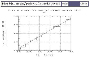
Select Measure/Simulate > Measure. The measured data should be similar to that shown in the following figure. The straight line is measured -Vc data. It should be fairly linear, and should only begin to deviate from a straight line at the high end of the base current value, if at all. If necessary, you can go back to the inputs and change the ib Stop value, then repeat the measurement. |
Figure 43 Example Measured rcflyback vcvsib Data
|
|
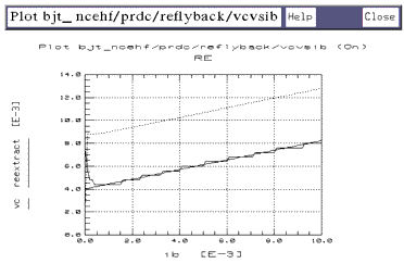
Making the reflyback Measurement
This procedure is similar to the rcflyback measurement. A current source drives the base to negate the effect of the base parasitic resistance. In this case the collector is open-circuited by setting its SMU current to zero. The change in collector voltage is monitored vs the change in base current. The collector voltage is the base current times the parasitic resistance in the emitter.
BJT Configuration: The input values you set in the following reflyback procedure configure the BJT as shown in the following figure.
Figure 44 BJT Configuration for reflyback Measurement
|
|
Parameters
The data from this measurement is used to extract the parasitic emitter resistance RE.
Defining the DC Source/Monitor Instrument State
Follow the same procedure you used in the fearly measurement. Use the same settings.
Setting the reflyback Input Values
| 1 |
Select the reflyback setup. |
| 2 |
Set the ib Start value to 0.000. Set Stop to a current value such that the measured Vc curve will be fairly linear. This is similar to the range used in the rcflyback measurement. |
| 3 |
Set the ic Sweep Type to CON (constant) with a Value of 0.000, to open-circuit the collector. |
Measuring and Plotting
| 1 |
From the Plots tab, select the vcvsib plot, and Display Plot. |
| 2 |
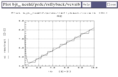
Select Measure/Simulate > Measure. The measured data should be similar to that shown in the following figure. Note that the stepped effect of the trace is caused by the resolution of the SMU in the DC source/monitor. |
Figure 45 Example Measured reflyback vcvsib Data
|
|
| 3 |
The Vc trace should be fairly linear, and should only begin to deviate from a straight line at the high end of the base current value, if at all. If necessary, go back to the inputs and change the ib Stop value, then repeat the measurement. |
Calibrating the Network Analyzer
It is important to calibrate the network analyzer before you perform any S-parameter measurements. Good calibration of the network analyzer is critical to a good measurement and extraction. Without a good calibration, the results of the extraction will be inaccurate.
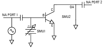
The high-frequency BJT measurement procedure requires a swept broadband calibration and one or two CW calibrations. The network analyzer is calibrated over the operating range of the device for the swept-frequency S-parameter measurements used to extract the AC device parameters. In addition, a calibration is performed at a single frequency for the CW S-parameter measurements used to extract the parasitic capacitance parameters. If the measurement system you are using is Agilent 8510-based, the CW calibration can be a subset of the broadband calibration. For Agilent 8753- and 8720- based systems, IC-CAP does not support the subset calibration technique, and separate standards measurements are needed for the swept and CW calibrations. In either case, a second CW calibration may be needed later for the h21vsvbe measurement.
CW Calibration Frequency
The frequency of the CW calibration for the capacitance measurements should be around 100 to 200 MHz to eliminate the effects of test set coupler roll-off at low frequencies, and low enough to eliminate bond inductance and other parasitic inductance considerations. With an Agilent 8510-based system, use a calibrated measurement point equal to the start frequency of the broadband cal plus an integer multiple of the step size: the frequency used in the example procedure is 110 MHz.
- 50 MHz (start freq) + 1 · 60 MHz = 110 MHz
The h21vsvbe measurement is also performed at a single CW frequency. However, this frequency is determined based on the data provided by the S-parameter measurements, and cannot yet be determined. When you reach the h21vsvbe measurement and determine the measurement frequency, you can use the same method to perform that calibration.
For step-by-step calibration procedures, refer to the appropriate chapter as follows:
Measuring the Junction Capacitances
The junction capacitances are measured with a calibrated network analyzer, rather than a CV meter, for the greatest measurement accuracy. Accurate capacitance measurements are extremely difficult at high frequencies, therefore the parasitic capacitance values are derived directly from the S-parameters measured at the collector and emitter of the device, with a CW frequency signal applied to the base.
Setting up the measurement conditions involves processes similar to those for the DC measurements: defining the instrument states and setting the inputs.
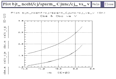
Making the sparm_Cjunc Measurement
This procedure measures the base-emitter and base-collector junction capacitances. An RF signal at a CW frequency is applied to the base, while the base voltage is swept from slightly forward-biased to strongly reverse-biased. A network analyzer takes S-parameter measurements from which the junction capacitances are derived.
|
Note
|
|
|
|
|
This setup combines and replaces both the earlier sparm_cje and sparm_cjc setups. While this simplifies the measurement, the bias is limited to the maximum base-emitter reverse breakdown voltage. If necessary, you can create two junction setups, sparm_cje and sparm_cjc, and make two separate measurements.
|
|
BJT Configuration: The input values you set in the following sparm_Cjunc procedure configure the BJT as shown in the following figure.
Figure 46 BJT Configuration for sparm_Cjunc Measurement
|
|
Parameters
The data from this measurement is used to extract CJE, VJE, MJE, CJC, VJC, and MJC.
Defining the Instrument States
Follow the steps described in the appropriate chapter shown next:
Set the Cal Set No to the cal set or register where you stored your CW calibration. The procedures in this manual use cal set #2. Then return to this chapter and continue.
Setting the sparm_Cjunc Input Values
| 1 |
Connect the network analyzer RF input cables to the RF IN ports of the bias networks. |
| 2 |
Select the sparm_Cjunc setup. |
| 3 |
The swept base voltage biases both the base-emitter and the base-collector junctions with the same voltage. The applied bias must be limited to the maximum base-emitter reverse breakdown voltage to prevent damage to the device. |
| 4 |
Set the vc Sweep Type to CON (constant) with a Value of 0.000, to open-circuit the collector. |
| 5 |
Do not change the ve values, which set the emitter to ground. |
| 6 |
Set the freq Sweep Type to CON (constant) to measure at a single CW frequency. |
| 7 |
Set the freq Value to the frequency of your CW calibration (see "Calibrating the Network Analyzer," earlier). The frequency used in this example procedure is 110 MHz. The frequency should be in the MHz range to eliminate the effects of test set roll-off at low frequencies, and low enough to eliminate bond inductance and other parasitic inductance considerations. |
|
Note
|
|
|
|
|
In setting a MHz value, write MEG in full. IC-CAP is not case-sensitive, and assumes that m or M corresponds to milli. If the message Error: NWA frequency value <45 MHz is displayed, you may have entered M only.
|
|
Measuring and Plotting
| 1 |
From the Plots tab, select the cj_vs_v plot, and Display Plot. |
| 2 |
Select Measure/Simulate > Measure. |
| 3 |
Save the data using File > Save As and a filename with the suffix .set. |
Measuring S-Parameters versus Frequency
The swept S-parameter measurements in the next two setups provide the data that allows extraction of parameters related specifically to the high-frequency performance of the device. The S-parameters are measured at the collector of the device, with a swept-frequency signal applied to the base. The first setup performs an S-parameter measurement without DC bias; the second is a DC-biased S-parameter measurement.
Making the sparm_0v Measurement
This procedure measures the S-parameters at the collector of the BJT across a calibrated microwave frequency range, with no DC bias signals applied.
BJT Configuration: The input values you set in the following sparm_0v procedure configure the BJT as shown in the following figure.
Figure 47 BJT Configuration for sparm_0v Measurement
|
|
Parameters
The data from this measurement will be used in the extraction of RB and LVIA.
Defining the Instrument States
Follow the steps described in the appropriate chapter shown next:
Note: The instrument states need to be set independently for each setup, and are different for CW and swept frequency measurements. Set the Cal Set No to the cal set or register where you stored your broadband calibration. The procedures in this manual use cal set #1. Then return to this chapter and continue.
Setting the sparm_0v Input Values
| 1 |
Select the sparm_0v setup. |
| 2 |
Set the Sweep Type for all the voltage inputs (vb, vc, and ve) to CON (constant), with a Value of 0.000, to apply zero bias at all terminals. |
| 3 |
Set the freq Sweep Type to LIN, for a linear measurement sweep across the frequency range. Set the Start and Stop values to correspond with the frequency range you defined in your broadband calibration. The frequency range used in the example procedure is 50 MHz to 6.05 GHz. Set the # of Points the same as in the calibration. |
Measuring and Plotting
| 1 |
From the Plots tab, select the s11 plot, and Display Plot. |
| 2 |
Select Measure/Simulate > Measure. The measured data should be similar to that shown in the following figure, though the trace may or may not cross the real (horizontal) axis. |
Figure 48 Example Measured sparm_0v s11 Data
|
|
The following steps determine the device resonant frequency Fr (the frequency where the S11 curve crosses the real axis), and the input impedance R(@Fr).
| 1 |
If the trace does not cross the real axis, you have two alternatives: |
| |
• |
You can increase the network analyzer upper frequency limit until the trace does cross the real axis (a time-consuming solution because you will need to recalibrate). |
| |
• |
Or (preferably) you can visually extrapolate the S11 trace to see where it would cross the real axis if it were actually extended. |
| 2 |
After you find the point where the trace crosses (or would cross) the axis, on the network analyzer press LOCAL to obtain front-panel control. Then press PARAMETER > S11 > FORMAT > SMITH CHART > MARKER > MARKER 1. Turn the RPG knob to move the marker to the point where the trace crosses the real axis. The marker readout shows the frequency at that point, as well as the real and imaginary impedance values. |
| 3 |
Record the frequency: this is the resonant frequency Fr of the device. |
| 4 |
Record the real impedance value: this is the input impedance R(@Fr). |
| 5 |
Save the measured data using File > Save As and a filename with the suffix .set. |
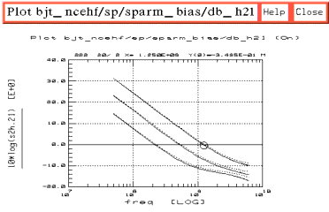
Making the sparm_bias Measurement
This procedure measures the S-parameters at the collector of the BJT across a calibrated microwave frequency range, at three values of base-emitter bias that take the device from near cutoff to near saturation.
BJT Configuration: The input values you set in the following sparm_bias procedure configure the BJT as shown in the following figure.
Figure 49 BJT Configuration for sparm_bias Measurement
|
|
Parameters
The data from this measurement will be used in the extraction of RB, IRB, RBM, TF, PTF, FC, and XCJC. This data will also be used to check the overall quality of all the extracted parameters.
Defining the Instrument States
Follow the steps described in the appropriate chapter shown next:
Use the same settings as you did for the sparm_0v setup. Then return to this chapter and continue.
Setting the sparm_bias Input Values
| 1 |
Select the sparm_bias setup. |
| 2 |
Set the vb # of Points to 3, to provide three different bias levels. |
| 3 |
To determine the Vb values, refer to the measured data from the fgummel measurement. Set vb Start to a value near device cutoff, and Stop to a value near saturation. |
| 4 |
Set the vc Sweep Type to CON (constant), with a Value at or near the normal operating point of the device. |
| 5 |
Do not change the ve values. |
| 6 |
Set the freq values the same as you did for the sparm_0v setup, to correspond with your broadband calibration. |
Measuring and Plotting
| 1 |
From the Plots tab, select Display All to display all the S-parameter plots. |
| 2 |
Select Measure/Simulate > Measure. Note that the db_h21 plot shows the device gain H21 at the three bias levels. |
| 3 |
If the db_h21 plot shows an unexpected drop in the gain of the device with bias (an abrupt change of several dB between one measurement point and the next), it is caused by thermal runaway. In this case, go back to the inputs and reduce the collector voltage by changing the vc Value. Then repeat the measurement. |
| 4 |
When you are satisfied with the measured data, save it using File > Save As and a filename with the suffix .set. |
Making the h21vsvbe Measurement
This procedure uses the network analyzer to measure H21 (the device current gain) versus Vbe, at a single microwave frequency. The base voltage is swept from near cutoff to near saturation. The H21 magnitude is derived from the S-parameters measured at the collector.
The measurement frequency is determined from the sparm_bias measurement data. A frequency is chosen in the linear range of the db_h21 plot. A network analyzer calibration is performed at that frequency prior to the h21vsvbe measurement, unless the frequency is the same as the frequency used for the sparm_Cjunc measurement.
Because this measurement data will be combined with the data from the ftic measurement performed next, the Vb and Vc values used in both measurements need to be identical. This is accomplished by setting input values for both procedures to variables that are defined in the model variables table, as explained below.
BJT Configuration: The input values and measurement variables you set in the following procedures configure the BJT as shown in the following figure.
Figure 50 BJT Configuration for h21vsvbe Measurement
|
|
Parameters
The data from this measurement and the ftic measurement will be used to generate Ft vs Ic. This will then be transformed to extract TF, VTF, XTF, and ITF.
Determining the Measurement Frequency
The frequency value for this measurement is determined from the sparm_bias measurement data.
| 1 |
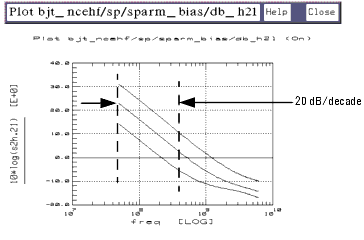
Referring to the db_h21 plot from your sparm_bias measurement, note that part of the trace has a roll-off of approximately 20 dB per decade. Within this portion of the trace, select a frequency near the low end (see Figure 51). |
| 2 |
To take advantage of the easy calibration subset capability of an Agilent 8510-based system, choose a frequency equal to the broadband cal start frequency plus an integer multiple of the calibration step size. Typically a frequency close to 200 MHz is adequate. The frequency used in the example procedure is 170 MHz. |
- 50 MHz (start freq) + 1 · 120 MHz = 170 MHz
- (If you have an Agilent 8753- or 8720-based system, you cannot use the cal subset feature with IC-CAP. Choose any appropriate frequency in the 20 dB per decade region of the trace.)
Figure 51 Determining the Frequency for the h21vsvbe Measurement
|
|
Calibrating the Network Analyzer
|
Note
|
|
|
|
|
If the frequency you selected for this measurement is the same as the frequency of the sparm_Cjunc measurement, you need not perform another calibration.
|
|
If the frequency you selected is not the same, and your system is Agilent 8510-based, perform the following steps to create a CW frequency calibration subset of the original broadband cal:
| 1 |
On the Agilent 8510 network analyzer, press CAL > CORRECTION ON > CAL SET 1 to turn on the broadband calibration. Then press MORE > MODIFY CAL SET > FREQUENCY SUBSET. |
| 2 |
Use the SUBSET: START and SUBSET: STOP softkeys in the subset menu (NOT the front panel keys) to set both start and stop to the same frequency. |
| 3 |
Press CREATE & SAVE, and store this calibration in cal set #3. |
If your system is Agilent 8753- or 8720-based and the frequency you selected is not the same as the frequency of the sparm_Cjunc measurement, perform a new CW calibration at that frequency.
Defining the Instrument States
Follow the steps described in the appropriate chapter shown next:
Use the same settings as you did for sparm_0v and sparm_bias, unless you performed a new calibration for this measurement, set Cal Set No to 3. Then return to this chapter and continue.
Setting the h21vsvbe Input Values
| 1 |
Select the h21vsvbe setup. |
| 2 |
Under vb, set Start to h21start, set Stop to h21stop, and set # of Points to h21npts. These are set to variables, instead of numerical values, to ensure the values will be identical to those used in the ftic measurement. The method for setting the actual values is described in the section, Defining the h21 Measurement Variables. |
| 3 |
Under vc, set Start to h21stop, so that the Vc start value equals the Vb stop value. Set Stop to a value close to the normal Vc operating point. However, if heat dissipation of the device fixture is a concern, keep the collector bias below 2V. |
| 4 |
Set the vc # of Points to 2, to measure at the lower and upper Vc values. |
| 5 |
Do not change the ve values. |
| 6 |
Set the freq Sweep Type to CONstant to measure at a single frequency. Set the Value to the frequency you defined at the beginning of this procedure. |
Defining the h21 Measurement Variables
This assigns numerical values to the variables listed as inputs. (The same values will apply to the ftic measurement.)
| 1 |
Select the Model Variables tab. The model variable table is displayed, as shown in the illustration. |
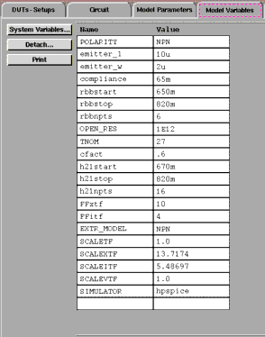
| 2 |
Set h21start and h21stop to appropriate Vbe values that will take the device from near cutoff to near saturation. The lower Vbe limit should not be so low that the device is cut off. The upper limit should be high enough that the measured H21 curve will begin to roll-off due to higher order effects. Typical values range from Vbe = 0.65V to 0.8V. |
| 3 |
Set h21npts (number of points) to a value that will make the voltage step size equal to an integer multiple of the Agilent 4142 voltage resolution. For information on the voltage resolution of Agilent 4142 SMUs, refer to the "Getting Started" chapter of the Agilent 4142B Operation Manual. |
Measuring and Plotting
| 1 |
Make the DUT/Setups folders active again and select the Plots tab. Select the h21_vbe plot, and Display Plot. |
| 2 |
Select Measure/Simulate > Measure. |
| 3 |
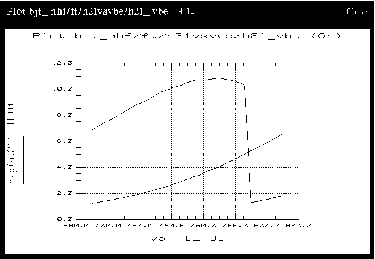
If the measured data shows an unexpected drop in magnitude (an abrupt change of several dB between one measurement point and the next), it is caused by thermal runaway. The following figure shows an example. In this case, go back to the variable table and reduce the upper limit of Vbe by reducing the h21stop value. Then repeat the measurement. |
Figure 52 Effects of Thermal Runaway
|
|
| 4 |
When you are satisfied with the measured data, save it using File > Save As and a filename with the suffix .set. |
Making the ftic Measurement
This is a DC-only measurement that monitors the change in collector current with respect to a change in base-emitter voltage. The device configuration is the same as for the h21vsvbe measurement, except there is no RF input signal.
Because this measurement data will be combined with the data from the h21vsvbe measurement performed previously, the Vb and Vc values used in both measurements need to be identical. For this reason, some of the input values are set as variables that were defined in the h21vsvbe procedure.
|
Note
|
|
|
|
|
The network analyzer test port cables can remain connected.
|
|
BJT Configuration: The input values you set in the following ftic procedure configure the BJT as shown in the following figure.
Figure 53 BJT Configuration for ftic Measurement
|
|
Parameters
The data from this measurement and the h21vsvbe measurement is used to generate Ft vs Ic. This is then transformed to extract TF, VTF, XTF, and ITF.
Defining the Instrument States
Follow the steps described in the appropriate chapter shown next:
Use the same settings as you did for the h21vsvbe setup.
Setting the ftic Input Values
| 2 |
Under vb, set Start to h21start, set Stop to h21stop, and set # of Points to h21npts, to ensure these values are identical to those used in the h21vsvbe measurement. |
| 3 |
Set vc Start to h21stop, so that the Vc start value equals the Vb stop value. |
| 4 |
Set vc Stop to the same value as in the h21vsvbe measurement. |
| 5 |
Set the vc # of Points to 2. |
| 6 |
Do not change the ve values. |
Measuring and Plotting
| 1 |
From the Plots tab, select the ft_ic plot, and Display Plot. |
| 2 |
Select Measure/Simulate > Measure. |
| 3 |
When you are satisfied with the measured data, save it using File > Save As and a filename with the suffix .set. |
Parameter Extraction
The extraction procedures are presented in the appropriate sequence to allow earlier extracted parameters to be used as a basis for later extractions.
In a BJT model, the parameters are very interdependent because of the inherent coupling of the model equations. The purpose of the different setups in the measurement process is to decouple the SPICE equations as much as possible. In the extraction process, the effects of individual parameters or small groups of related parameters can be isolated, and their values determined with reasonable certainty. The goal is to create a list of realistic parameters that can be used in a model to accurately predict device performance. Because of the interdependence of the parameters, the extraction process is extremely iterative, and involves many subjective judgments. The validity of the extracted parameters must be checked repeatedly.
The ability to discern reasonable values from questionable ones comes from knowledge of device physics, familiarity with a particular device, and individual experience. Parameter extraction is very much an art.
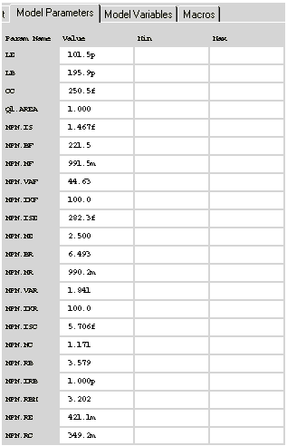
Displaying the Parameters Table
The bjt_ncehf Model Parameters table lists all the parameters that will be extracted, and initially displays default values. As you perform the individual extractions, the default values change to extracted values. Throughout the extraction process, you will use the Parameters table to read extracted values, and to enter or modify values to adjust interactive parameters for best agreement of simulated with measured data.
| 1 |
Click the Model Parameters tab. The table of model parameters is displayed, showing the current values of the individual parameters. The illustration shows a portion of the table. |
Figure 54 Top Portion of the Model Parameters Table
|
|
| 2 |
To save the Parameters table after your device parameters are extracted, select File > Save As. |
| 3 |
In the dialog box, select the File Type .mps for model parameter set. |
| 4 |
Type a filename or use the one in the File Name field and click OK. |
You can now recall the same set of device parameters any time you wish.
Extracting the Junction Capacitance Parameters
This procedure extracts the base-emitter parameters CJE, VJE, and MJE; and the base-collector parameters CJC, MJC, and VJC. These parameters are extracted from the data measured in the sparm_Cjunc setup.
|
|
CJE
|
Zero-bias base-emitter capacitance.
|
VJE
|
Base-emitter junction built-in potential.
|
MJE
|
Base-emitter grading coefficient.
|
CJC
|
Zero-bias base-collector capacitance.
|
VJC
|
Base-collector junction built-in potential.
|
MJC
|
Base-collector grading coefficient.
|
| 1 |
Scroll the Parameters table until it shows the values for CJE, VJE, and MJE. |
| 2 |
Select DUT/Setups > sparm_Cjunc. |
| 3 |
From the Plots tab, select the cj_vs_v plot, and Display Plot. |
Figure 55 Measured and Simulated sparm_Cjunc cj_vs_v Data
|
|
| 4 |
Select the Extract/Optimize tab. |
| 5 |
Select the set_Cjunc transform, and Execute. The transform calculates the values for CJE and CJC and enters them in the Parameters table. |
| 6 |
Select calc_cje > Execute. Then select opt_cje > Execute. The simulated cje data in the plot should converge on the measured data, as in the previous figure. |
| 7 |
Select calc_cjc > Execute. Then select opt_cjc > Execute. The simulated cjc data in the plot should converge on the measured data. |
Extracting the Collector Parasitic Resistance RC
This procedure extracts RC, using the data measured with the rcflyback setup. The measurement drives the base with a current source to negate the effects of the base parasitic resistance, and monitors -Vc vs Ib with Ie at 0 amps. The measured value at Vc is therefore equal to Ib times RC.
| 1 |
Select the rcflyback setup. |
| 2 |
Select Plots > vcvsib > Display Plot. The plotted -Vc voltage is the product of the base current times the collector parasitic resistance (see the following figure). |
Figure 56 Example Plotted rcflyback vcvsib Data
|
|
| 3 |
Select the Extract/Optimize tab. |
| 4 |
Select the rcextract transform, and Execute. The transform calculates RC as the slope of the -Vc vs Ib curve, and enters the value in the Parameters table. |
Extracting the Emitter Parasitic Resistance RE
This procedure is similar to the previous one. It extracts RE, using the data measured with the reflyback setup. The measurement drives the base with a current source to negate the effects of the base parasitic resistance, and monitors Vc vs Ib with Ic at 0 amps. The measured value at Vc is therefore equal to Ib times RE.
| 1 |
Select the reflyback setup. |
| 2 |
Select Plots > vcvsib > Display Plot. The plotted collector voltage is the product of the base current times the emitter parasitic resistance (see the following figure). |
Figure 57 Example Plotted reflyback vcvsib Data
|
|
| 3 |
Select Extract/Optimize > reextract > Execute. The transform calculates RE as the slope of the Vc vs Ib curve, and enters the value in the Parameters table. |
The Intrinsic and Extrinsic Inductances
The intrinsic inductances of high-frequency BJTs are usually relatively small. At the frequencies where a BJT is normally used, they have essentially no effect on the device model. Compared to extrinsic parasitic inductance values such as the bond inductances, the intrinsic inductance values are small enough that they can be ignored.
A greater effect is caused by the extrinsic bond inductances LB and LE. In addition, if a carrier is used that has a via hole connecting the emitter pad to the backside ground plane, an additional amount of inductance is inherent in the via. This parasitic inductance is LVIA: its value is added to the value of LE.
The next procedure records the values for LB and LE; the following procedure extracts LVIA where applicable.
The Bond Inductances LB and LE
For this step it is necessary that the base and emitter bond inductances of your device are known. For example, if you know the inductance per unit length of the bond wire used, you can calculate the total bond wire inductance. Be sure to minimize the bond inductances, by making the bond length as small as possible or the bond wire as thick as possible.
| 1 |
Scroll the Parameters table until it shows the parameters LB and LE. |
| 2 |
Manually enter the base and emitter bond inductance values for your device. |
Extracting LVIA and RB
In a device mounted in a carrier that has a via hole connecting the emitter pad to the backside ground plane, LVIA is the inductance of the via. RB is the zero-bias base resistance.
|
Note
|
|
|
|
|
If you are making on-wafer probed measurements rather than in-fixture measurements, you can ignore the effects of LVIA (but not of RB).
|
|
This procedure uses data from the sparm_0v measurement to solve two equations. At zero bias the input of a BJT can be modeled as a series RLC circuit, where:
- R = RE + RB
L = LE + LB + LVIA
C = CJE0
(Note that this ignores the effects of CJC0 and the BJT output circuit. The resultant error for a typical high-frequency device with an fT of >4 GHz is <10%.)
| 1 |
From the sparm_0v measurement, note the values you recorded for the device resonant frequency Fr and the input impedance R(@Fr). |
| 2 |
Refer to the Parameters table for the value of RE you extracted earlier. |
| 3 |
Use a calculator to find the value of RB by solving this equation: |
- RB = R(@Fr) - RE
| 4 |
Manually enter the calculated value for RB in the Parameters table. |
| 5 |
If applicable, use the previously recorded values for LB and LE to find the value of LVIA by solving this equation: |
- LVIA = [CJE · (2 ·
 · Fr)2]-1 - (LB + LE) · Fr)2]-1 - (LB + LE)
| 6 |
Add the value of LVIA to the value of LE in the Parameters table, and manually enter the total into the Parameters table as the new value for LE. |
Extracting VAR and VAF
This procedure is very iterative. The values for both VAR (the reverse early voltage) and VAF (the forward early voltage) are strongly dependent on the saturation current IS. The value of IS, however, is in turn strongly dependent on VAR. Therefore, the procedure begins with a first-pass rough extraction of IS, which is used in the extractions of VAR and VAF. After the values of VAR and VAF are extracted and optimized, IS will be extracted again using these values, in the next procedure.
First Estimate of IS
| 1 |
Select the fgummel setup. |
| 3 |
Select Extract/Optimize > isextract > Execute. The transform calculates a first estimate value for IS and enters it in the Parameters table. |
Extracting VAR
| 1 |
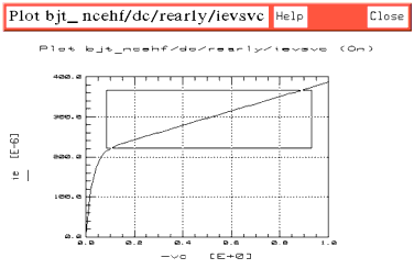
Select the rearly setup. |
| 2 |
Select Plots > ievsvc > Display Plot. The plotted data should be similar to Figure 59. |
| 3 |
Select Extract/Optimize > evextract > Execute. This calculates a first estimate of both VAR and VAF. |
| 4 |
The VAR extraction will be optimized over only the linear portion of the Ie trace. The next steps use the X-low/X-high function to select a portion of the trace. |
| |
• |
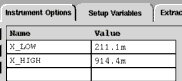
Select the Setup Variables tab. A variable table will appear, listing X_LOW and X_HIGH with their current values, as shown in the illustration. |
Figure 58 The rearly Setup Variables Table
|
|
| |
• |
From the plotted data choose a linear portion of the Ie trace, along the constant slope of the saturated region (as illustrated by the box in Figure 59). Avoid any curved area at the high end of the trace. Click the mouse pointer at the lower and upper boundary points of the linear portion to make a box on the trace. |
| |
• |
From the plot menu select Options > Copy to Variables. This changes the X_LOW and X_HIGH values for this plot to your boundary points. |
| 5 |
Select Extract/Optimize > opt_var > Execute. The transform converges the simulated data to the measured data in the plot. It calculates the value of VAR using the linear portion of the Ie trace you defined with X-low/X-high, and enters the value in the Parameters table. |
Figure 59 Plotted rearly ievsvc Data for VAR Extraction
|
|
Extracting VAF
This is similar to the procedure for VAR, using the fearly setup.
| 1 |
Select the fearly setup. |
| 2 |
Select Plots > icvsvc > Display Plot. |
| 3 |
Use the X-low/X-high function to define a linear portion of the Ic trace for the extraction, as explained under Extracting VAR. |
| 4 |
Select Extract/Optimize > opt_vaf > Execute. The transform converges the simulated data to the measured data. It calculates the value of VAF using the portion of the trace you defined, and enters the value in the Parameters table. |
Extracting IS, NF, BF, ISE, NE, and IKF
This procedure uses several different transforms that isolate and optimize the individual parameters in the regions where they have the most dominant effect. These forward parameters are all extracted using the data measured with the fgummel setup. Note that extractions based on the fgummel measurement make the assumption that Ic = -(Ie + Ib).
Table 19 Forward parameters extracted using the fgummel setup
|
|
IS
|
Transport saturation current.
|
NF
|
Forward current emission coefficient (models the deviation of the emitter-base diode junction from the ideal).
|
BF
|
Ideal maximum forward beta.
|
ISE
|
Base-emitter leakage saturation current (the value of the base current at zero base-emitter voltage).
|
NE
|
Base-emitter leakage emission coefficient (models the recombination of the base current in the base-emitter space charge region at low base-emitter voltage).
|
IKF
|
Forward knee current (models the drop in forward beta at high collector currents due to high-level injection).
|
Initial Extraction
| 1 |
Select the fgummel setup. |
| 2 |
Select Extract/Optimize > isextract > Execute to extract initial values for IS and NF. |
| 3 |
Select fgextract > Execute to extract initial values for IKF, BF, ISE, and NE. |
| 4 |
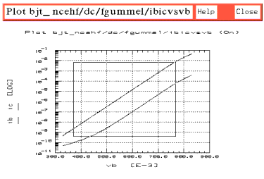
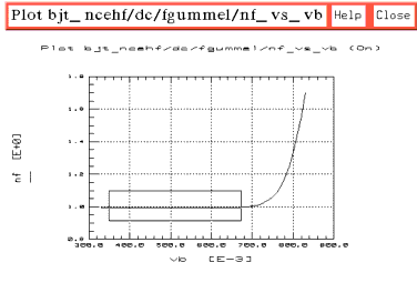
Select Plots > ibicvsvb > Display Plot, and nf_vs_vb > Display Plot. |
| 5 |
Select Measure/Simulate > Simulate. |
| 6 |
Observe the plots. The simulated data should be reasonably close to the measured data. If so, proceed to "Optimizing IS and NF." |
| 7 |
If the simulated data does not match fairly well with the measured data, the optimizer may not converge properly. In this case, extract the parameters manually with the Draw Diag Line feature, using the "Manual Extractions" explanations at the end of this procedure. Then come back to the optimization procedures given below. |
Optimizing IS and NF
This optimization is performed over a section of the Ic curve at medium Vbe values, avoiding the low and high current effects.
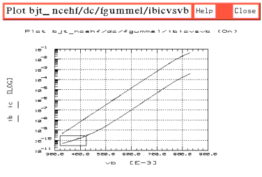
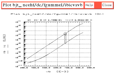
| 1 |
Using the ibicvsvb plot (Figure 60), choose a section of the Ic (upper) curve at medium Vbe values. Avoid the low and high current effects. Alternatively, use the nf_vs_vb plot and choose a Vbe range where NF is reasonably flat and near minimum (see Figure 61). |
Figure 60 Appropriate Region of Ic for Optimization of IS and NF
|
|
| 2 |
Use the X-low/X-high function to define the section of the curve to be optimized: |
| |
• |
Position the pointer at the lower end of your chosen range and click left, then at the high end and click left. |
| |
• |
From the plot menu select Options > Copy to Variables, to change the X-low/X-high values to the trace limits you selected. |
| 3 |
Select Extract/Optimize > optic_is_nf > Execute. The transform converges the simulated data to the measured data in the plot. It optimizes the values for IS and NF using the section of the curve you defined, and enters the values in the Parameters table. |
Figure 61 Appropriate NF Region to Optimize IS and NF
|
|
Optimizing BF
| 2 |
Select opt_beta > Execute. The transform optimizes the value for BF using the defined section of the Ic curve, and enters the value in the Parameters table. |
Optimizing ISE and NE
This optimization is performed at the low end of the Ib curve.
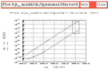
| 1 |
Using the ibicvsvb plot, choose a section at the low end of the Ib curve where the slight bending upward of the trace indicates the recombination in the base-emitter depletion region. Refer to Figure 62: the portion of the trace in the box is the appropriate region for optimization. |
Figure 62 Appropriate Region of Ib for Optimization of ISE and NE
|
|
| 2 |
Use the X-low/X-high function to define the section of Ib to be optimized. |
| 3 |
Select optib_ise_ne > Execute. The transform converges the simulated data to the measured, and enters the optimized values for ISE and NE in the Parameters table. |
Optimizing IKF
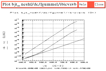
This optimization is performed at the high end of the Ib and Ic curves.
| 1 |
Using the ibicvsvb plot, choose a section at the high end of both curves where they begin to deviate from a straight line. Refer to Figure 63: the portion of the traces in the marked box is the appropriate region for optimization. Alternatively, look at the nf_vs_vb plot (Figure 61), and set the lower limit for optimization above the point where NF begins to deviate from a straight line. The upper limits for Ic and Ib are set by the maximum value of Vb. |
Figure 63 Appropriate Region of Ib and Ic for Optimization of IKF
|
|
| 2 |
Use the X-low/X-high function on one of the traces, to define the range to be optimized. |
| 3 |
Select opt_ikf > Execute. The transform converges the simulated data to the measured, and enters the optimized value for IKF in the Parameters table. |
Manual Extractions (Optional)
Use these procedures only if the data simulated in Initial Extraction does not match reasonably well with the measured data.
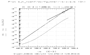
Manually Extracting IS and NF
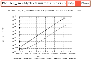
| 1 |
Use the ibicvsvb plot. Choose a linear portion of the Ic vs Vb curve, avoiding the low and high current effects. Put the mouse pointer at the low end of the chosen portion and click left, then put the pointer at the high end and click left, to make a box on the trace. |
| 2 |
From the plot menu select Options > Draw Diag Line. A diagonal line is drawn on the plot that extends the linear portion you chose to the boundaries of the plot (see the following figure for an example). Annotations below the plot give the values for: |
- Slope of the diagonal line
Yo, the y-axis intercept of the diagonal line
Xo, the x-axis intercept of the diagonal line
| 3 |
Manually enter the Yo value into the Parameters table as the value for IS. |
Figure 64 Manual Extraction of IS and NF Using Draw Diag Line
|
|
| 4 |
Solve the following equation (using a calculator) to determine the value of NF. Note that this equation is only valid up to high injection effects. |
-
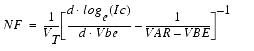
- where:

- and:
- elementary charge q = 1.60218 · 10-19
- Planck's constant k = 1.38066 · 10-23
- temperature T = TNOM + 273.15
| 5 |
Manually enter the NF value in the Parameters table. |
Manually Extracting BF
| 1 |
Using the ibicvsvb plot, pick a value of Vb in the linear portion of the Ib and Ic curves where the curves are as close as possible to parallel. The following figure shows an example. |
Figure 65 Manual Extraction of BF
|
|
-
 where both Ic and Ib are measured at the same Vb.
| 2 |
To determine the value of Ic at the chosen value of Vb, position the pointer on the trace at that value, and click middle to get a readout of the value at that point. |
| 4 |
Subtract the logarithmic value of Ib from the logarithmic value of Ic to get the value of BF. |
| 5 |
Manually enter the value of BF in the Parameters table. |
Manually Extracting ISE and NE
| 1 |
Using the ibicvsvb plot, choose a linear portion at the low end of the Ib vs Vb curve, where the slight bending upward of the trace indicates the recombination in the base-emitter depletion region. |
| 2 |
Use the Draw Diag Line feature to extrapolate the linear portion to the boundaries of the plot (the following figure shows an example). |
Figure 66 Manual Extraction of ISE Using Draw Diag Line
|
|
| 3 |
Read the Yo value from the annotations below the plot, and manually enter it in the Parameters table as the value for ISE. |
| 4 |
Use a calculator to solve the following equation for NE. Note that this equation is only valid at low Vbe values where recombination takes place in the base-emitter space charge region. |
-
- where:

- and:
- elementary charge q = 1.60218 · 10-19
- Planck's constant k = 1.38066 · 10-23
- temperature T = TNOM + 273.15
| 5 |
Manually enter the NE value in the Parameters table. |
Manually Extracting IKF
A hardcopy plot is used for this procedure.
| 1 |
Choose File > Print from the ibicvsvb plot, to obtain a hardcopy of the plot. |
| 2 |
Manually draw a diagonal line along the linear portion of the Ic curve in the medium range of Vbe. Extend the line beyond the trace at the top end, as illustrated. |
| 3 |
Draw another diagonal line along the upper range of Ic where the high-level effects begin to dominate. Extend the low end of the diagonal line so that it intersects the first diagonal line, as in the following figure. |
| 4 |
IKF is the value of IC at the intersection of the two diagonal lines. Put the mouse pointer on the trace at this point, and click middle to get a readout of the value. |
| 5 |
Manually enter the value of IKF in the Parameters table. |
Figure 67 Manually Extracting IKF
|
|
Verifying the Manual Extractions
| 1 |
Select Measure/Simulate > Simulate. |
| 2 |
Observe the ibicvsvb plot. The simulated and measured data should now be very close. |
| 3 |
Now go back to Optimizing IS and NF. Perform that and the subsequent three procedures for optimizing BF, ISE and NE, and IKF. |
| 4 |
Close the ibicvsvb plot. |
Extracting NR, BR, ISC, NC, and IKR
The procedure for extracting these reverse parameters corresponds closely to the last procedure for extracting the forward parameters. The main differences are that IS is not extracted in the reverse direction, and that the rgummel data is used in place of the fgummel. As in the forward gummel extractions, this procedure uses several different transforms that isolate and optimize the individual parameters in the regions where they are most dominant. Note that extractions based on the rgummel measurement make the assumption that Ie = -(Ic + Ib).
Table 20 Reverse parameters extracted using the rgummel setup
|
|
NR
|
Reverse current emission coefficient (models the deviation of the collector-base diode junction from the ideal).
|
BR
|
Ideal maximum reverse beta.
|
ISC
|
Base-collector leakage saturation current (the value of the base current at zero base-collector voltage).
|
NC
|
Base-collector leakage emission coefficient (models the recombination of the base current in the base-collector space charge region at low base-collector voltages).
|
IKR
|
Reverse knee current (models the drop in reverse beta at high emitter currents due to high-level injection).
|
Initial Extraction
| 1 |
Select the rgummel setup. |
| 2 |
Select Extract/Optimize > nrextract > Execute to extract the initial value for NR. |
| 3 |
Select rgextract > Execute to extract initial values for BR, ISC, NC, and IKR. |
| 4 |
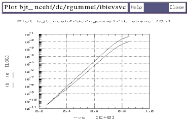
Select Plots > ibievsvc > Display Plot. |
| 5 |
Select Measure/Simulate > Simulate. |
| 6 |
Observe the ibievsvc plot. The simulated data should be reasonably close to the measured data. If so, proceed to "Optimizing NR." |
| 7 |
If the simulated data does not match fairly well with the measured data, the optimizer may not converge properly. In this case, extract the parameters manually with the Draw Diag Line feature, as explained for the forward gummel parameters under Manual Extractions (Optional). Then come back to the optimization procedures given below. |
Optimizing NR
This optimization is performed over a section of the Nr curve at medium Vce values, avoiding the low and high current effects.
| 1 |
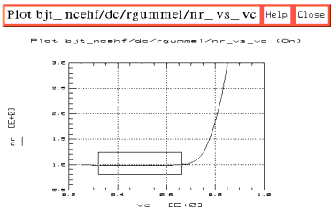
Select Plots > nr_vs_vc > Display Plot. |
| 2 |
Choose a linear section of the curve at medium Vce values, as shown in the following figure. Avoid the low and high current effects. |
Figure 68 Appropriate Region of Trace for Optimization of NR
|
|
| 3 |
Use the X-low/X-high function to define the section of the curve to be optimized: |
| |
• |
Position the mouse pointer at the low end of your chosen range and click left, then at the high end and click left. |
| |
• |
From the plot menu select Options > Copy to Variables, to change the X-low/X-high values to the trace limits you selected. |
| 4 |
Select Extract/Optimize > optie_nr > Execute. Observe the ibievsvc plot (Figure 69) to see the simulated Ib and Ie data converge to the measured data. The transform optimizes the value for NR using the section of the trace you defined, and enters it in the Parameters table. |
Figure 69 Measured and Simulated Ib and Ie Data, Well Converged
|
|
Optimizing BR
| 2 |
Select opt_beta > Execute. The transform optimizes the value for BR using the defined section of the trace, and enters the value in the Parameters table. |
Optimizing ISC and NC
This optimization is performed at the low end of the curve.
| 1 |
Using the nr_vs_vc plot, choose a section at the low end of the curve, as in the following figure. If possible, look for a transitional area where the slope begins to change, indicating the recombination in the base-collector space charge region. |
Figure 70 Appropriate Region of Curve for Optimization of ISC and NC
|
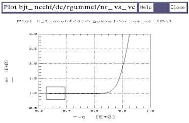
|
| 2 |
Use the X-low/X-high function to define the section of the curve to be optimized. |
| 3 |
Select optib_isc_nc > Execute. The transform converges the simulated data to the measured, and enters the optimized values for ISC and NC in the Parameters table. |
Optimizing IKR
This optimization is performed over the upper portion of the Nr curve.
| 1 |
Using the nr_vs_vc plot, choose a section at the high end of the measured curve starting with the transitional area where the slope begins to change. Refer to Figure 71: the portion of the trace in the box is the appropriate region for optimization; the upper limit is set by the maximum value of Vc. |
Figure 71 Appropriate Region of Trace for Optimization of IKR
|
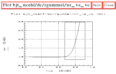
|
| 2 |
Use the X-low/X-high function to define the section of the trace to be optimized. |
| 3 |
Select optie_ikr > Execute. The transform converges the simulated data to the measured, and enters the optimized value for IKR in the Parameters table. |
Verifying the Predicted DC Performance
All the DC parameters have now been extracted. Before you proceed to the AC parameter extractions, it is important to verify that the extracted parameters do indeed predict the DC performance of the device. The AC performance of the device, and hence the AC extractions, are strongly dependent on the accuracy of the DC parameters.
Comparing the Measured and Resimulated fearly Data
| 1 |
Select the fearly setup. |
| 2 |
Select Plots > icvsvc > Display Plot. |
| 3 |
Select Measure/Simulate > Simulate. |
| 4 |
Observe the plot. The resimulated data using the new parameters should be almost indistinguishable from the measured data. |
Comparing the Measured and Resimulated rearly Data
| 1 |
Select the rearly setup. |
| 2 |
Select Plots > ievsve > Display Plot. |
| 3 |
Select Measure/Simulate > Simulate. |
| 4 |
Observe the plot. Due to the non-reciprocal nature of the base-emitter and base-collector junctions, the current levels of the measured and simulated rearly data will not coincide. SPICE assumes that the saturation current IS is identical for both junctions: since this is not in reality the case, it is seldom possible to have both the fearly and rearly data match simultaneously. However, the slope of the Ic vs Vce curve beyond saturation is independent of IS, and therefore the measured and simulated slopes should match in this region. |
Comparing the Measured and Resimulated fgummel Data
| 1 |
Select the fgummel setup. |
| 2 |
Select Plots > ibicvsvb > Display Plot. |
| 3 |
Select Measure/Simulate > Simulate. |
| 4 |
Observe the plot. Even though the equations describing the forward gummel data are dominated by the forward gummel parameters, the reverse parameters do also have an effect. Therefore check that the forward gummel data resimulated using the new parameters still closely matches the measured data. |
Modifying the DC Parameters
You may obtain unexpected results from your comparisons between measured DC data and data resimulated using the new parameters. In this case, you might choose to make minor changes in the values of one or more parameters, to more closely match the simulated data to the measured data. If you do this, it is important that you check all the DC simulations, and modify other parameters if necessary, to compensate. This cycle must be continued until all simulations are acceptable, and you will probably have to make some trade-offs in the process. You will need to exercise judgment based on your knowledge of device physics and the particular device under test.
AC Extractions
The AC performance of the device, and hence the AC extractions, are strongly dependent on the accuracy of the DC parameters. It is essential that the DC parameters and the parasitic capacitance and resistance parameters are known to be good, before the AC extractions are done. If you have any doubts about the validity of these parameters, continue to refine the DC extractions before proceeding with the AC extractions.
Setting Initial Values for FC and XCJC
The final values for FC and XCJC will be extracted after the other AC parameters have been determined. Because FC and XCJC have an effect on the overall AC performance of the device, initial values are assigned to them before extraction of the other parameters.
| • |
If you know the values of FC and XCJC for your device, enter those values into the Parameters table. |
| • |
If you do not know the values of FC and XCJC for your device, enter the value of FC as 0.5, and the value of XCJC as 0.7. |
Extracting High-Frequency Transit Time Parameters
This procedure uses several different transforms to optimize the individual parameters in the regions where they have the most dominant effect. The parameters are extracted using both the h21vsvbe and ftic setups.
Table 21 Parameters extracted using the h21vsvbe and ftic setups
|
|
TF
|
Ideal forward transit time (models the finite bandwidth of the device in forward mode).
|
XTF
|
Bias-dependence coefficient of TF (models the minimum value of TF at low Vce and high Ic).
|
VTF
|
Voltage describing the dependence of TF on Vbc (models the effects of Vbc on TF).
|
ITF
|
High-current parameter effect on TF (models the decline of TF with high Ic).
|
Initial Extraction
| 1 |
Select the h21vsvbe setup. |
| 2 |
Select Measure/Simulate > Simulate. |
| 4 |
Select Plots > ft_ic > Display Plot. |
| 5 |
Select Extract/Optimize > Ft > Execute to draw the Ft vs Ic data on the plot. |
| 6 |
Select AC_decoupled > Execute. The transform calculates the values for TF, XTF, VTF, and ITF, and enters them in the Parameters table. |
| 7 |
If the simulated curves do not converge closely to the measured curves, you can perform manual optimization procedures using the h21vsvbe setup, starting on the next page. The procedures make iterative changes to the values in the Parameters table to obtain a best fit of the simulated curves to the measured curves. |
Optimizing TF and VTF
This is an iterative process that optimizes the convergence of the simulated data at the peaks of the curves. TF sets the height of both peak values of Ft (the peaks of both Vce curves). VTF sets the separation between the two curves at their peak Ft value.
| 1 |
Select Model Parameters. In the Parameters table, modify the values of both TF and VTF. These are "first guess" value changes that will be modified iteratively until you achieve acceptable results. |
| 2 |
Select DUT/Setups > h21vsvbe. |
| 3 |
Select Plots > h21_vbe > Display Plot. |
| 4 |
Select Measure/Simulate > Simulate. |
| 5 |
Observe the plot. The simulated curves should match the measured curves reasonably well at the peaks of both Vce curves, as in the following figure. |
Figure 72 Measured and Simulated Vce Curves (Ft vs Ic)
|
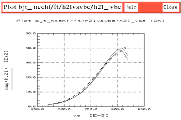
|
| 6 |
If not, repeat the above steps as necessary to modify the TF and VTF values and resimulate, until the simulated and measured curves at both values of Vce are close at the point where Ft is maximum. |
Optimizing ITF
This is an iterative process that optimizes the simulated data for the high end of the Ic curves. ITF predominantly affects the high Ic roll-off of the lower Vce curve, and also has an appreciable effect on the higher Vce curve.
| 1 |
In the Parameters table, modify the value of ITF. This is a "first-guess" value change. |
| 2 |
Select the h21vsvbe setup. |
| 3 |
Select Measure/Simulate > Simulate. |
| 4 |
Observe the ft_ic plot from the ftic setup. The simulated curves should match the measured curves reasonably well in the region of high Ic roll-off. |
| 5 |
If not, repeat as necessary to improve the convergence of the simulated data to the measured data in the region of high Ic roll-off, especially in the lower curve. |
Optimizing XTF
This optimizes the convergence of the simulated data for the upper Vce curve. XTF value changes should be minimal.
| 1 |
After ITF is set, sparingly modify the value of XTF in the Parameters table. |
| 2 |
In the h21vsvbe setup select Measure/Simulate > Simulate. |
| 3 |
Observe the ft_ic plot. The upper simulated Vce curve should converge to the upper measured curve. |
| 4 |
If not, repeat as necessary until the curves converge. |
Extracting PTF
This procedure uses the H21 magnitude data measured in the sparm_bias setup to determine the value of PTF, the excess phase of TF (which is also the value of excess phase at Ft).
| 1 |
Select the sparm_bias setup. |
| 2 |
Select Plots > db_h21 > Display Plot. |
| 3 |
In the db_h21 plot, find the highest frequency where the H21 magnitude is 0 dB (see the following figure). If necessary, use the Draw Diag Line feature to extend the highest Vbe curve through the 0 dB line. |
Figure 73 Determining Ft. Example Plot of H21 Magnitude
|
|
| 4 |
Position the pointer on the trace at this point and click middle to get a readout of the values. The frequency (x-axis value) at that point is Ft. |
| 5 |
Select the ph_h21 plot, and Display Plot. Figure 74 illustrates a typical H21 phase plot. |
| 6 |
Find the location of Ft on the ph_h21 plot. Put the mouse pointer on the trace at this point and click middle to get a readout of the phase value. |
- Solve for PTF by subtracting 90° from the phase of H21 at Ft:
- PTF (degrees) = |phase of H21 @ Ft| -90
| 7 |
Manually enter the calculated value of PTF in the Parameters table. |
Figure 74 Typical Plot of H21 Phase, with Location of Ft
|
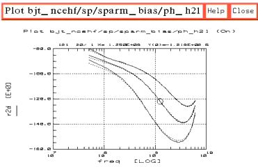
|
Extracting IRB and RBM
This procedure uses the S11 data measured in the sparm_bias setup to extract the following parameters:
Table 22 Parameters extracted using the sparm_bias setup
|
|
IRB
|
Current where the base resistance falls halfway to its minimum value from its zero-bias value RB.
|
RBM
|
Minimum base resistance at high currents (models the effects of current crowding on the base resistance).
|
| 1 |
In the sparm_bias setup, select the s11 plot, and Display Plot. |
| 2 |
Select Measure/Simulate > Simulate. Observe the high-bias S11 curve on the plot. If the measured and simulated values agree at the resonant frequency (where the S11 curve crosses the real axis), no adjustment of RBM is needed. If the high-bias S11 curve does not cross the real axis, visually extrapolate to see where it would cross the real axis if it were extended: if measured and simulated values agree no adjustment of RBM is needed. |
| 3 |
If the high-bias measured and simulated S11 values do not agree at the resonant frequency (or the extrapolated resonant frequency), modify the value of RBM in the Parameters table. This is a "first guess" value change. |
| 4 |
Select Measure/Simulate > Simulate. |
| 5 |
Continue to modify the value of RBM and resimulate until the measured and simulated values of S11 do agree at the resonant frequency. |
| 6 |
Observe the medium-bias S11 curve on the plot. If the measured and simulated values agree at the resonant frequency, no adjustment of IRB is needed. |
| 7 |
If the medium-bias measured and simulated S11 values do not agree at the resonant frequency, modify the value of IRB in the Parameters table and resimulate. |
| 8 |
Continue to modify the value of IRB and resimulate until the measured and simulated values do agree at the resonant frequency. |
| 9 |
The simulated low-bias S11 curve depends mainly on the value of RB extracted earlier, and should therefore already agree with the measured value. |
Extracting CC
This procedure uses the S22 data measured in the sparm_bias setup to extract CC, the parasitic capacitance at the output of the device. This represents the capacitance between ground and the pad on which the device is epoxied, as well as any other stray capacitance to ground. This value is very difficult if not impossible to measure directly, therefore its value is determined indirectly using the following method.
| 1 |
In the sparm_bias setup select the s22 plot, and Display Plot. |
| 2 |
If the maximum frequency points (end points) of the measured and simulated S22 curves are comparable in value, no adjustment of CC is needed. |
| 3 |
If the maximum frequency points of the measured and simulated S22 curves are not comparable in value, modify the value of CC in the Parameters table. This is a "first-guess" value change. |
| 4 |
Select Measure/Simulate > Simulate. |
| 5 |
Continue to modify the value of CC and resimulate until the maximum frequency points of the measured and simulated curves are comparable in value. |
Extracting FC
This procedure uses the data measured in the ftic setup to extract FC, the coefficient for forward bias capacitance. The S11 data measured in the sparm_bias setup is also used to verify the value of FC.
FC models the continuity between the forward and reverse bias base-emitter capacitance. Therefore it has the most effect at the low end of the Vbe curves, in the region dominated by junction capacitances where the base-emitter junction capacitance is comparable to the forward diffusion capacitance.
| 2 |
Select Plots > ft_ic > Display Plot. |
| 3 |
The simulated data should match the measured data reasonably well at the low end of the curves, in the region indicated in the following figure. |
Figure 75 Region of Curves Where Junction Capacitances Dominate
|
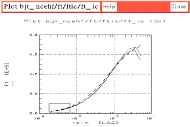
|
| 4 |
If the simulated data does not match the measured data in the indicated region, modify the value of FC in the Parameters table. |
| 5 |
Select Measure/Simulate > Simulate. |
| 6 |
Continue to modify the value of FC and resimulate until the simulated data converges to the measured data in the indicated region. |
| 7 |
Select the sparm_bias setup. |
| 8 |
Select Plots > s11 > Display Plot. |
| 9 |
Check the convergence of the simulated to measured S11 curves in the low-bias region. If they are well converged, this verifies that the extracted value of FC is good. |
| 10 |
Leave the s11 plot open. |
Extracting XCJC
This procedure uses the S11 and S22 data measured in the sparm_bias setup to extract XCJC, the fraction of base-collector capacitance connected to the internal base node. XCJC models the distributed effects of the base-collector junction. The effects are typically only noticeable at high frequencies.
| 1 |
In the sparm_bias setup select the s22 plot, and Display Plot. |
| 2 |
The simulated data should match the measured data at the higher frequencies. |
| 3 |
If not, modify the value of XCJC in the Parameters table. |
| 4 |
Select Measure/Simulate > Simulate. |
| 5 |
Repeat as necessary to improve the convergence of the simulated to measured S11 and S22 curves at the higher frequencies. |
Final Parameter Adjustments
All the BJT parameters have now been extracted. To verify the accuracy of the AC parameters, now resimulate all the AC setups using the final parameters. It may be necessary to make minor modifications to one or more of the parameters to achieve a better fit between the simulated and measured data. This is a somewhat nebulous task: the following instructions are guidelines that try to provide some structure. None of the parameters should require more that slight adjustment: if any of them do, some of the parameter values may be suspect.
Recall that the DC, capacitance, and parasitic resistance parameters have a significant influence on the simulated AC performance of the device. Therefore, if it is difficult or impossible to find AC parameters that adequately predict the AC performance, it may be necessary to modify some or all of these parameters. Note that, because of the inherent interaction between parameters, any change to one usually requires the modification of many. If too many parameters need to be modified by too much, it may be advisable to start the extraction process over.
LE, LB and LVIA
Use the S-parameter plots in the sparm_bias setup, starting with s11. Cautiously adjust the values of these parameters in the Parameters table and resimulate, until the simulated S-parameter curves match the measured ones. The values of the parasitic inductance parameters vary the length of the curves, particularly the S11 curves. This is because of the BF+1 factor in the impedance transformation from emitter to base, which causes the inductances at the emitter to have much more of an effect on the input impedance, and consequently on S11.
RC
Use the s22 plot in the sparm_bias setup. Cautiously adjust the value of RC in the Parameters table and resimulate, until the simulated S22 curves match the measured ones. The effect of RC is most prominent at the high-frequency end of the S22 curves. Varying RC affects the loss of S22, therefore the value of RC can be adjusted until the high-frequency ends of the simulated and measured S22 curves line up.
TF
Use the h21_vbe plot in the h21vsvbe setup. Adjust the value of TF in the Parameters table and resimulate, to improve the match between the peaks of the simulated and measured curves.
XCJC and FC
The requirements for extracting these parameters are less rigid than for other more explicitly defined parameters. Therefore, you can modify either or both of these values in the Parameters table to adjust the overall simulated AC performance if necessary.
RE
Use the s11 plot in the sparm_bias setup. Although RE has been determined through the DC extraction using the reflyback data, you may need to adjust its value slightly to accommodate the AC performance. You can do this by monitoring the simulated loss in the S11 curves. Note that in a fashion identical to LE the effect of RE on the input impedance is increased by the factor BF+1. This results in S11 being very sensitive to RE, especially at bias values where BF is large. Be very careful when you adjust this parameter!
IS and NF
Be particularly careful here. These two parameters have a dramatic effect on the overall performance of the device. If, during the course of fine-tuning the final parameter values, you decide to adjust either IS or NF, you will need to perform the extraction process again, based on the new values for IS and NF.
Storing the Model
This procedure stores the model in IC-CAP, including all the device-specific measured and simulated data. Once you have developed the device model, it can be used as a component in the Agilent RF and Microwave Design System (MDS). You can use it for circuit simulation, inserting it into circuits under design to emulate the characteristics of your device.
If you will be modeling large numbers of devices, it is worthwhile to organize your directory structure according to device type, geometry, and batch or wafer.
| 1 |
Use the directory you created at the beginning of the procedure, when you first opened the bjt_ncehf.mdl file. |
| 2 |
From the bjt_ncehf:1 main menu select File > Save As. |
| 3 |
A dialog box is displayed, as illustrated. |
Figure 76 Save As Dialog Box
|
|
| 4 |
Select the File Type (.mdl for a complete model) by clicking the corresponding radio button. |
| 5 |
Select a new filename that associates this model with the device, for example bjt3.mdl. Type the full directory pathname and the filename into the dialog box. Select OK to store the data and close the dialog box. |
|