Using the EEFET3/EEHEMT1 Example Model Files
This chapter provides a sequence of example procedures that take you step-by-step through a FET or HEMT measurement and extraction. The procedures are arranged in the proper sequence to allow earlier measured data or extracted parameters to be used as a basis for later measurements or extractions. The extraction is the same for a FET or a HEMT, except that the additional parameters used for a HEMT can be omitted in a FET extraction.
A series of different IC-CAP setups are used to measure current, voltage, or S-parameters vs. bias under different bias and frequency conditions. The model parameters are then extracted from the various sets of measured data.
|
Note
|
|
|
|
|
These procedures measure the device in a common-source configuration.
|
|
Macros automate the modeling procedure so that a series of similar devices can be modeled quickly with minimal user intervention, although you can execute individual transforms for specific measurement and parameter extractions.
The detailed procedures (executing individual transforms) in this chapter include instructions for the following:
| • |
Performing a set of device preview measurements and setting measurement variable values based on the results. |
| • |
Setting the hardware instrument states and input variables for each measurement. |
| • |
Making the parasitic, DC, and S-parameter measurements: qualifying the results. |
| • |
Extracting and optimizing the individual model parameters. |
| • |
Verifying the extraction results against the measured data. |
Where appropriate, other chapters are cross-referenced, so that all system hardware setups and calibrations are performed at the right times.
|
Note
|
|
|
|
|
Measurement parameters and measured data are specific to individual devices. Information and data are provided here as examples and guidelines, and are not intended to represent the only correct method or results.
|
|
The procedures start with example values for the model variables. They provide guidelines on setting the values to measure your own devices. However, the values you use will be based on your knowledge of your FET/HEMT devices or on information provided by the device vendors, as well as on the guidelines presented here: they may or may not correspond with the examples. In some cases, it may be necessary to set the variable values for the preview measurements, make a measurement, and then reset the variables based on the measurement results. The procedures give suggestions on judging the applicability of the variable values and the measured data.
The illustrations of plotted data are provided as visual examples of possible measurement and simulation results. They are not intended to represent a sequential measurement and extraction of a single device, nor do they necessarily correspond with the example measurement inputs and variable values in the procedures. The plots can be used to check the reasonableness of your own data, which should appear similar in shape but not necessarily coincident in values.
In addition, the IC-CAP software itself includes measured data for some of the setups. This data shows additional examples of possible results. Many, though not all, of the input settings for this measured data correspond with the example settings in this manual.
The DUTs and Setups
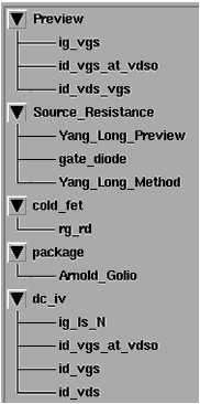
The DUT/Setup panel is part of the Model window, which is the central access point for all the individual measurement and modeling procedures.The Model window includes tabs to access the macros, the Model Parameters table, and other IC-CAP features. To open this model, click the Examples button on the toolbar and locate /model_files/mesfet/HPEEfet3.mdl.
Figure 108 Portion of the Agilent EEFET3/EEHEMT1 DUT/Setup Panel
|
|
In the DUT/Setup panel the DUTs (for example Preview)—indicated by the inverted triangles—are groupings of similar measurement setups used for related measurements and extractions. The setups (for example ig_vgs) contain the information used to define the inputs and outputs for each measurement, as well as their measurement hardware configurations and their associated transforms and plots.
The measurement and parameter extractions are most easily performed with macros. If you use macros, you will not need to use the individual setups. However, if you want to extract individual parameters or "fine-tune" a parameter, you will use the individual setups. (Note that you can also write macros to control other repetitive tasks, using IC-CAP's Parameter Extraction Language, PEL.)
ReadMe is not actually a macro, but an abbreviated version of the instructions in this chapter. It is most appropriate for users who are somewhat familiar with the model. You can view the Readme file in a separate window by clicking Detach. You can then resize the window and move it away from the central work area. Scroll through the text as you work through the model.
Model Parameters
The tables in this section describe the various parameters and list their default values.
Drain-Source Current Parameters
The drain-source current model was developed through examination of Ids, as well as drain-source conductance (Gds) and transconductance (Gm), vs. bias plots on a wide class of devices from various manufacturers. The model assumes the device is symmetrical, and therefore is valid for values of Vds < 0.0 V as well as Vds > 0.0 V. The parameters in the following table are extracted from drain-source current measurements:
Table 36 Drain-Source Current Parameters
|
|
|
Vto
|
Zero-bias threshold parameter.
|
-1.5 (V)
|
Gamma
|
Vds-dependent threshold parameter.
|
0.05 (1/V)
|
Vgo
|
Gate-source voltage where transconductance is maximum.
|
-0.5 (V)
|
Vdelt
|
Parameter that controls linearization point for Gm characteristic.
|
0.0 (V)
|
Vch
|
(Vchannel) Gate-source voltage where Gamma no longer affects the I-V curve.
|
1.0 (V)
|
Gmmax
|
Peak transconductance parameter.
|
70.0e-3 (S)
|
Vdso
|
Drain voltage where Vds dependency disappears from equations.
|
3.0 (V)
|
Vsat
|
Drain-source current saturation parameter.
|
1.0 (V)
|
Kappa
|
Output conductance parameter.
|
0.0 (1/V)
|
Peff
|
Channel-to-backside self-heating parameter (effective power compression).
|
2.0 (W)
|
Vtso
|
Subthreshold onset voltage.
|
-10.0 (V)
|
Charge Parameters
The gate charge model was developed through examination of extracted device capacitances over bias. The capacitance data is obtained from measured Y-parameter data in the saturation region.
Table 37 Charge Model Parameters
|
|
|
C11o
|
Maximum input capacitance for Vds=Vdso and Vdso>Deltds.
|
0.3 (pF)
|
C11th
|
Minimum (threshold) input capacitance for Vds=Vdso.
|
0.03 (pF)
|
Vinfl
|
Inflection point in C11-Vgs characteristic.
|
-1.0 (V)
|
Deltgs
|
C11th to C11o transition voltage.
|
0.5 (V)
|
Deltds
|
Linear region to saturation region transition parameter.
|
1.0 (V)
|
Lambda
|
C11-Vds characteristic slope parameter.
|
0.05 (1/V)
|
C12sat
|
Input transcapacitance for Vgs=Vinfl and Vds>Deltds.
|
0.03 (pF)
|
Cgdsat
|
Gate-drain capacitance for Vds>Deltds.
|
0.05 (pF)
|
Ris
|
Source-end channel resistance.
|
2.0 (ohms)
|
Rid
|
Drain-end channel resistance.
|
0.0 (ohms)
|
Tau
|
Source-to-drain charging delay.
|
1.0 (ps)
|
Cdso
|
Drain-source inter-electrode capacitance.
|
80.0 (fF)
|
Dispersion Parameters
Dispersion parameters are extracted from measured S-parameter data, to provide additional accuracy for dispersion effects at higher frequencies. The dispersion parameters listed in the table below are optimized to measured transconductance (Gm) data to model both DC and RF dispersion characteristics. Similarly, the dispersion parameters are optimized to measured output conductance (Gds) data.
Table 38 Dispersion Model Parameters
|
|
|
Rdb
|
Dispersion source output impedance.
|
1.0e9 (ohms)
|
Cbs
|
Dispersion source capacitance.
|
1.6e-13 (F)
|
Gdbm
|
Additional d-b branch conductance at Vds=Vdsm.
|
0.0 (S)
|
Kdb
|
Parameter that controls Vds dependence of additional d-b branch conductance.
|
0.0 (dimensionless)
|
Vdsm
|
Voltage where additional d-b branch conductance becomes constant (Gdbm).
|
1.0 (V)
|
Gmmaxac
|
Peak transconductance parameter (AC).
|
60.0e-3 (S)
|
Vdeltac
|
Parameter that controls linearization point for Gm characteristic (AC).
|
0.0 (V)
|
Vtoac
|
Zero-bias threshold parameter (AC).
|
-1.5 (V)
|
Gammaac
|
Vds-dependent threshold parameter (AC).
|
0.05 (1/V)
|
Kappaac
|
Output conductance parameter (AC).
|
0.0 (1/V)
|
Peffac
|
Channel-to-backside self-heating parameter (AC).
|
10.0 (W)
|
HEMT Gm Compression Parameters
Some FETs and almost all HEMTs exhibit transconductance compression in which Gm peaks and then decreases. The following parameters model these compression effects.
Table 39 Additional Parameters Used in EEHEMT1 for Gm Compression
|
|
|
Vco
|
Voltage where transconductance compression begins.
|
10.0 (V)
|
Mu
|
Parameter that adds Vds dependence to transconductance compression onset.
|
0.0 (dimensionless)
|
Vba
|
Transconductance compression "tail-off" parameter.
|
1.0 (V)
|
Vbc
|
Transconductance roll-off to tail-off transition voltage.
|
1.0 (V)
|
Deltgm
|
Slope of transconductance compression characteristic.
|
0.0 (S/V)
|
Alpha
|
Transconductance saturation-to-compression transition parameter.
|
1.0e-3 (V)
|
Calibrating the Network Analyzer
All the EEFET3/EEHEMT1 S-parameter measurements require only one calibration: a swept broadband calibration across the operating frequency range of the device under test. Good calibration of the network analyzer is critical to a good measurement and extraction.
For step-by-step calibration procedures, refer to:
| • |
Wiltron 360 network analyzer—Refer to the Wiltron documentation |
Make the following additional setting changes:
| • |
Set the frequency range for the calibration to the range you intend to use for your measurements, at least as wide as the operating range of the device. |
| • |
Set the network analyzer START frequency to the lowest possible frequency in the range of the network analyzer and bias networks: low frequencies allow more accurate AC conductances to be extracted. The example procedure in the software uses 50 MHz. |
| • |
Set the STOP frequency to the upper limit of the frequency range for the device under test. Frequencies up to Ft are useful but not required. Good package and charge extractions require frequencies high enough to see roll-off and package effects clearly. The example procedure uses 3 GHz. |
| • |
Set the NUMBER of POINTS to 51 or 101 to provide clear and usable S-parameter plots: more points only add more time and memory requirements to the measurement and extraction. |
Remember these frequency values: you will also need to enter them in IC-CAP when instructed. If you do not set these values correspondingly, the calibration will be invalid.
All S-parameter measurements for the EEFET3/EEHEMT1 model are performed over the same frequency range.
|
Note
|
|
|
|
|
If you set a MHz value in IC-CAP, write MEG in full. IC-CAP is not case-sensitive and assumes that m or M corresponds to milli. If an error message is displayed during the measurement that indicates a network analyzer frequency value is too low, you may have entered M only.
|
|
Remember the number of the network analyzer cal set or register where you store the calibration. You will need to use this number in the instrument options of each S-parameter measurement setup when you define the instrument states.
Using Macros for Measurements and Extractions
Macros automate the modeling procedure so that a series of similar devices can be modeled quickly with minimal user intervention. As a macro is run, it sets the control and device measurement variables in the model variable table usually needed for the extraction procedure being run. The control variables are explained in the next pages. These are the macros and their purposes:
Table 40 Macro Descriptions
|
|
Set_Measurement_Ranges
|
Execute the device preview (including Yang_Long_Preview) and initialization steps, setting all the control variables.
|
Package_extraction_only
|
Measure the data from which the package parasitics are extracted, and perform the extractions.
|
DC_extraction_only
|
Makes the DC measurements and performs the DC extractions.
|
AC_extraction_only
|
Makes the S-parameter measurements and performs the AC extractions.
|
Measure_all_data
|
Executes all measurements
|
Extract_all_parameters
|
Extracts model parameters based on existing data
|
Measure_and_Extract_ALL
|
Performs a complete device measurement and extraction using the measurement ranges recorded in the model variable table
|
Xtract
|
Performs the parameter extraction procedure. Called by all the other macros except Set_Measurement_Ranges.
|
Macro Sequence
One possible appropriate sequence for performing the macros is as follows:
| 2 |
Package_extraction_only |
| 3 |
DC_extraction_only (and study the results) |
| 4 |
AC_extraction_only (and study the results) |
Control Variable Flags in the Macros
Control variable flags are set to 1 or 0 in the macros to simplify operation and customize the macros. Each macro starts with default values for the control variables, so they can be used as is or modified to meet your needs. For details, refer to Running the Macros.
Table 41 Macro Control Variables
|
|
|
control_view
|
Displays the plots.
|
Suppresses the plots.
|
control_measure
|
Performs the measurements.
|
Skips the measurement steps. Used with previously- stored data.
|
control_extract
|
Executes the parameter extraction.
|
Skips the parameter extraction.
|
control_package
|
Executes the package extraction.
|
Skips the package extraction.
|
control_dc_model
|
Executes the DC measurement and extraction.
|
Skips the DC procedures.
|
control_ac_model
|
Executes the AC measurement and extraction.
|
Skips the AC procedures.
|
control_save
|
Saves a Series IV compatible file.
|
Does not save a Series IV compatible file.
|
The control variables can also be set in the variable table, but control variable values set in the macros override variable table values.
To see more detail on the macro flags, you can select any macro to read the contents of the macro.
Running the Macros
| 1 |
In the Model window, select the macro of your choice. |
| 2 |
To change control variable flags (see Table 42), use Back Space or Delete and replace the current value with a different value. |
|
Note
|
|
|
|
|
If you want to see the control variable values change when you execute the macro, Detach the model variable table.
|
|
| 3 |
To start the macro, click Execute. The macro will start to run. You can see the control variable values change in the model variable table if you have modified them in the macro. |
| 4 |
If you select the Set_Measurement macro, you will be prompted to enter values for certain variables. Otherwise the variable table default values are used. Note that the variable values must be appropriate to the particular device being modeled, or the macro results will not be valid. |
|
Note
|
|
|
|
|
You will need to know several things about the device under test to supply appropriate values. For example, you will be prompted for the device gate width and length. You also need to supply certain voltage or current values. Some of these values can be found in the device manufacturer's data sheet. The list of device input variable values later in this chapter also lends insight into appropriate values for different variables. Default values are also available, and may be appropriate for use in many cases.
|
|
- The macro will set numerical values for the control and device measurement variables (see Table 42) needed for the measurement and extraction procedure being run. Then the macro will perform the required measurement and extraction procedures.
- If you have the control_view flag set to 1, you will see the measured and extracted data plotted on the screen.
- When the macro is complete, the results of the extraction are displayed in the Status window.
Device Input Variable Values
One of the first requirements in performing the EEFET3/EEHEMT1 modeling procedures is to set numerical values for the model variables. When executing the macros, you are prompted for several variable values. Other variables are calculated by the software based on your input. The Set_Measurement_Ranges macro is especially useful in establishing initial settings in preparation for a complete extraction. We recommend that you use this macro for initialization of the model variable table.
Model Variables
The EEFET3/EEHEMT1 model variables are described in the following table.
Table 42 EEFET3/EEHEMT1 Model Variables
|
|
CAP_FACTOR
|
Used as a scaling factor in setting charge parameter optimzation limits.
|
CHECK_DATA
|
Used in the macros to control extent of application/user interface. Typically opens plots and performs transforms for visual inspections.
|
control_ac_model
|
Used in the macros to control the AC measurement and extraction procedures. 1 performs the procedures, 0 does not.
|
control_dc_model
|
Used in the macros to control the DC measurement and extraction procedures. 1 performs the procedures, 0 does not.
|
control_doc
|
Not used in this Model.
|
control_expert
|
Used to control the level of interaction between the application and the user. 1 non verbose, 0 verbose.
|
control_extract
|
Used in the macros to control the parameter extraction steps. 1 executes the extraction, 0 skips the extraction.
|
control_frequency
|
Used in Set_Measurement Macro to set input responses which guide the user in determining whether or not to initialize Frequency settings and Instrument Options for Network Analyzer (NWA). 1 to guides the user through NWA settings, 0 does not.
|
control_hemt
|
Determines whether the device will be modeled as a FET or a HEMT. It is normally set to 1 for a HEMT, and 0 for a FET. However, the HEMT setting generally works well with standard MESFETs also, providing a better Gm curve fit. In particular, it is suggested you use the HEMT setting for a device where the Gm curve peaks and then rolls off as Vgs becomes more positive.
|
control_measure
|
Used in the macros to control the measurement steps. 1 performs the measurements, 0 suppresses the measurements.
|
control_package
|
Used in the macros to control the package parasitics measurement and extraction procedures. 1 performs the procedures, 0 does not.
|
control_save
|
Used in the macros to save a Series IV compatible file. 1 saves the file, 0 does not.
|
control_view
|
Used in the macros to control display of the plots. 1 displays the plots, 0 suppresses the plots.
|
control_YL_method
|
Used in Xtract macro to guide the extraction process. Also used in the method for selecting Rs. 1 selects Yang Long method, 0 does not.
|
FC
|
The frequency at which the charge model is extracted. Use a frequency value that gives about 90 degrees of rotation of the S-parameters measured.
|
FG
|
The frequency at which device conductances are extracted. Experience has shown that data just above the trap effects is the best for extraction of conductances.
|
FREQ_POINTS
|
The number of points for S-parameter measurements. This must be the same as the number of points set for the network analyzer calibration. 51 or 101 provides clear and usable S-parameter plots: more points only add more time and memory requirement to the measurement and extraction.
|
FREQ_START
|
The start frequency of the network analyzer for S-parameter measurements. Use the lowest possible frequency in the range of the network analyzer and bias networks: low frequencies allow more accurate AC conductances to be extracted. This must be the same as the start frequency set for the network analyzer calibration. (See "Calibrating the Network Analyzer," later in this chapter.)
|
FREQ_STOP
|
The stop frequency of the network analyzer for S-parameter measurements. This should be the upper limit of the frequency range for the device under test, and must be the same as the stop frequency set for the network analyzer calibration. Frequencies up to Ft are useful but not required. Good package and charge extractions require frequencies high enough to see rolloff and package effects clearly.
|
FS
|
The frequency at which Tau and Ri are extracted. It must be about where S11 crosses the real axis: this is the point where the impact of the device parasitics causes the least problem.
|
I_RES
|
The current resolution of the power supply being used. This value is used in macros to help truncate current limits to values that do not violate the resolution limits of the DC power supplies in use.
|
Id_per_Wg_factor
|
An empirical based scaling factor used for preliminary determination of Wg (gate Width) or IDSS, Set_Measurment Macro.
|
ID0_MAX_SUPPLY
|
Used in determining if Power Supply limits have been or will be exceeded.
|
ID1_MAX_SUPPLY
|
Used in determining if Power Supply limits have been or will be exceeded.
|
ID2_MAX_SUPPLY
|
Used in determining if Power Supply limits have been or will be exceeded.
|
ID3_MAX_SUPPLY
|
Used in determining if Power Supply limits have been or will be exceeded.
|
IDS_FACTOR
|
Use as a scaling factor for setting the optimization range of DC-IV equation parameters: gmmax, vgo, vto etc.
|
IDS_MAX
|
The compliance limit for Ids values. (The Agilent 41420A high-power SMU likely to be connected to the device drain has a maximum output current of 1.0A. A standard Agilent 11612A option K10/K20 bias network has a maximum input current of 0.5A.)
|
IDS_NOM
|
The intended Ids of device operation.
|
IDS_VTO_FACTOR
|
The fraction of the maximum drain current that will define the drain current at Vto.
|
IDS_VTO_MAX
|
Calculated value of Ids a Vto. (2 * IDS_VTO_MAX)
|
IDS_VTO_MIN
|
Calculated value of Ids at Vto.
|
IDS_YL_MAX
|
The upper limit of Ids used to extract Rs. It also will be different for every transistor type and size. You will select this value from the data plot presented by the Yang_Long_Preview measurement. The value must be within 10% of IDS_YL_MIN.
|
IDS_YL_MIN
|
The lower limit of Ids used to extract Rs. It will be different for every transistor type and size. You will select this value from the data plot presented by the Yang_Long_Preview measurement. The value must be within 10% of IDS_YL_MAX. Remember to use values within the settability limits of the DC source/monitor.
|
IDS_YL_PTS
|
The Yang_Long method requires swept measurements of two slightly different values of drain current, therefore the standard number of Ids points is 2.
|
IDSS_ACTUAL
|
Used to store value of Idss from measured data. Also used in calculations of other variables. In some cases IDSS_ACTUAL is assigned the value IDSS_DATA_SHT.
|
IDSS_DATA_SHT
|
The Idss value for the device. This may be specified in a manufacturer's data sheet. If you do not know an expected value for Idss, you can use the default value.
|
Ig_density
|
The gate current density of the device, typically 50x106 A/m2. The software uses the gate width and length values, in combination with the gate current density, to calculate safe forward gate bias levels.
|
IG_FWD_IV
|
This is the maximum allowable DC gate current. This value is used to measure VG_FWD_IV, which in turn is used to set the value of VGS_MAX, the highest Vgs used in swept bias measurements.
|
IG_FWD_MAX
|
This is the gate current at VG_FWD_MAX, and should be slightly less than the critical gate current IFwd but high enough to reduce the gate diode's dynamic resistance to a few ohms. It is used in the ig_vgs device preview setup.
|
IG_FWD_MID
|
This is a current about 95% of the value of IG_FWD_MAX. It is used to measure VG_FWD_MID.
|
IG_FWD_MIN
|
This is a current about 95% of the value of IG_FWD_MID. It is used to measure VG_FWD_MIN.
|
IG_FWD_RATIO
|
The percent reduction of Ig from IG_FWD_MAX to IG_FWD_MID to IG_FWD_MIN. It is usually approximately 92% to 98% as specified by Dambrine and Cappy for their method of extracting Rg and Rd.
|
IG_MAX
|
Not used in this model.
|
IGS_MAX
|
The compliance limit for Igs values. The default value, 0.100A, is the maximum output current of the Agilent 41421B medium-power SMU likely to be connected to the device gate. You provide compliance values to limit SMU output current or voltage and prevent damage to the device under test, as well as to the SMUs, bias networks, and probes if used.
|
IGS_YL_MAX
|
Select this value in the linear region of the Yang_Long_Preview plot, at the upper end of the region, and where the Igs value is between 50 and 100 times smaller than the maximum Ids value selected.
|
IGS_YL_MIN
|
For the Rs extraction Vgs is measured between IGS_YL_MIN and _MAX. Like the Ids values, you will select the Igs values from the data plot presented by the Yang_Long_Preview measurement. Select an IGS_YL_MIN value in the linear region of the plot, near the lower end, and where the Igs value is between 50 and 100 times smaller than the minimum Ids value selected.
|
IGS_YL_PTS
|
The number of Igs points used in the Rs extraction measurement. Remember in setting these last three Igs values to use limits and number of points values that result in steps within the settability limits of the DC source/monitor: the steps will be within uA spacing.
|
Lg
|
The gate length of the device, in microns.
|
MEASURE_FAST
|
Not used in this model.
|
model_file_name
|
This is used to define the disk file name.
|
model_name
|
Current name of model. Used in macro to specify iccap path (example: model_name > DUT > Setup > Plot)
|
Pdiss_MAX
|
Maximum safe power dissipation of the device. This is used to check the VDS_MAX value once Idss is known.
|
RANGE_FACTOR
|
Used to adjusts the limits of optimization for the dynamic IV parameter set.
|
Rch_factor
|
Not used in this model.
|
SIMULATOR
|
not used in this model.
|
TOL_VOLT
|
Not used in this model.
|
TOL_FUNC
|
Not used in this model.
|
TRACE_MAX
|
This sets an upper limit for the optimization range of Vds for the gm_gds optimization in the AC_all DUT.
|
TRACE_MIN
|
This sets a lower limit for the optimization range of Vds for the gm_gds optimization in the AC_all DUT.
|
V_RES
|
The voltage resolution of the power supply being used. This value is used in macros to help truncate voltage limits to values that do not violate the resolution limits of the DC power supplies in use.
|
V_RES_vto
|
Used to set the correct resolution for Vgs.
|
VD1_MAX_SUPPLY
|
Used in determining if Power Supply limits have been or will be exceeded.
|
VD2_MAX_SUPPLY
|
Used in determining if Power Supply limits have been or will be exceeded.
|
VD3_MAX_SUPPLY
|
Used in determining if Power Supply limits have been or will be exceeded.
|
VDELT_FACTOR
|
Used as a scaling factor when scaling the parameter EEFET3.vdelt.
|
VDS_COARSE
|
The number of Vds points used for making DC-biased S-parameter measurements. A number between 5 and 15 results in a good extraction.
|
VDS_FINE
|
The number of Vds points used in gate characterization steps. 51 points is an adequate number.
|
VDS_MAX
|
The largest safe Vds value for all Vgs values. Be aware of the power dissipation limits of your device at high Ids levels, to prevent damage to the device.
|
VDS_MIN
|
The smallest value of Vds. This is usually 0.0V, but may be a negative value.
|
VDS_NOM
|
The intended Vds of device operation.
|
VDS_YL_LMT
|
The maximum allowable Vds for Rs measurement and extraction.
|
VDS_YL_MAX
|
The Rs extraction must be done at Vds values less than 0.25V. This guarantees the extraction takes place in the region of linear transistor operation. Use a value at the upper end of the linear region. These Vds values generally will never have to be changed except in the case of a device with a very sharp knee.
|
VDS_YL_MIN
|
This is the lower limit of the Vds range for the Rs extraction, which must be done at Vds values less than 0.25V. Use a value in the linear region, near the low end of the region.
|
VDSO
|
A Vds value just above the knee in full saturation. This is the point where the model equations simplify, and is an important operating characteristic for most GaAs FETs. Manufacturers often specify Idss at values of Vds that generally work well as Vdso settings. Vdso=3.0V is a good default that will nearly always work.
|
VG_FWD_IV
|
A measured Vgs value where a normally small forward quiescent DC gate current flows for an active bias condition. It is used to help determine VGS_MAX for DC and AC measurements.
|
VG_FWD_MAX
|
The upper limit of Vgs at VDS_ZERO for the rg_rd cold fet measurement.
|
VG_FWD_MID
|
VG_FWD_MID is the gate voltage used to produce IG_FWD_MID.
|
VG_FWD_MIN
|
This is the lower limit of Vgs with Vds at VDS_ZERO, used to measure S-parameters at forward gate bias in the parasitic resistance measurement.
|
VG_FWD_PTS
|
The number of points for the rg_rd measurement. This is the number of measurements you wish to make between VG_FWD_MIN and VG_FWD_MAX, inclusively. Three points are sufficient.
This following series of _YL_ variables are all used in the Yang_Long measurements from which the parasitic source resistance Rs is extracted. It is highly recommended that the initialize transform be used to set these values once the Yang_Long_Preview measurement is made. The preview measurement is based on voltages that are nearly universally applicable. The initialize transform extracts the highly device-dependent currents needed to use this method of extracting RS. Refer to the procedures later in the chapter.
|
VG_GML_MAX
|
The largest Vgs value used for Gummel measurements. Since this data is not used to extract contact resistances, use values that yield Igs values  IFwd/2. IFwd/2.
|
Note Remember that the Agilent 4142 DC source/monitor and its SMUs are limited in the ability to set and resolve voltage steps. In all cases where a measurement will be stepped over a number of points, set values that will make the voltage step size equal to an integer multiple of the Agilent 4142 voltage resolution. Voltage steps in fractional mV settings are not valid and will not work. The "Getting Started" chapter of the Agilent 4142B Operation Manual has more information on the voltage resolution of Agilent 4142B SMUs.
|
VG_GML_MIN
|
The smallest gate characterization voltage, used for Gummel measurements. Data taken over this range is used in the gate diode and source resistance extractions. Values lower than about 0.2V to 0.3V result in Igs data that is indistinguishable from noise.
|
VG_GML_RANGE
|
A minimum difference allowed between VG_GML_MAX and VG_GML_MIN, usually 0.5V. It helps to keep the gate characterization measurements within a linear, noise-free range.
|
VGO_FACTOR
|
Used to initialize the parameter EEFET3.vgo.
|
VGS_COARSE
|
The number of Vgs points used for making DC-biased S-parameter measurements. S-parameters will be measured at each of these bias points at every calibrated frequency point. If the VGS_COARSE number of points is specified too large, more data than necessary will be taken and the measurement will take an excessive amount of time. A number between 5 and 15 results in a good extraction.
|
VGS_FINE
|
The number of Vgs points used in gate characterization steps. 101 points is an adequate number. Remember that voltage steps in fractional mV increments do not work.
|
VGS_MAX
|
The highest (most positive) Vgs value where the device can be operated quiescently at VDS_MAX.
|
VGS_MIN
|
A Vgs value that gives even, easy-to-use steps and is more negative than the device pinchoff voltage at VDS_NOM.
|
VGS_NOM
|
The value of Vgs that gives an Ids value representative of actual device operation.
|
VGS_YL_MAX
|
The Vgs compliance for the Yang_Long_Method. This protects the device from overdrive on the gate. A value of 0.6V will work for nearly all devices used, though occasionally it may need to be set to 0.7V.
|
VTO_FACTOR
|
Not used in this model.
|
Wg
|
The gate width of the device, in microns.
|
YL_IdIg_RATIO
|
The factor used to compute acceptable gate currents as a function of drain current in Yang and Long's source resistance method. Usually between 50 and 100.
|
Executing Individual Measurement Transforms
While the macros are appropriate for measuring and modeling devices for which the device type is well known, you may prefer to set the variable values yourself rather than have them set by the macros. Or situations may occur where the device is not known and you need to perform the device measurements separately and extract the parameters individually from the measured data.
When executing individual transforms, you will sometimes be prompted to supply variable values. You will also input some variable values directly in the model variable table.
The rest of this chapter explains in detail how to:
| • |
Make preview device measurements and set the model variables from the results obtained |
| • |
Make the measurements required for specific extractions |
| • |
Perform the individual extractions |
| • |
Save the resulting model |
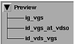
The Preview DUT
The Preview DUT contains three setups, as shown in the following illustration:
These setups are used to obtain a good set of measured DC-IV curves on which most of the other measurements will be based. In performing these measurements, you set the variable values to define the measurement limits. Some values are selected to protect a device from damage. Other values cause data to be taken over a wide enough range to ensure usable model results, or taken in specific regions of interest to you.
Begin with anticipated reasonable values depending on your knowledge of the device under test. Then modify the values as necessary until you are satisfied with the measurement results.
The validity of the later measurements and the accuracy of the model are dependent on obtaining a good set of preview measurements. Note, however, that when extracting many devices of the same type, repeated device preview is not necessary.
|
Note
|
|
|
|
|
The Set_Measurement_Ranges macro performs all the steps outlined here. A thorough understanding of what is done in these steps and how it fits into the extraction methodology will make the extraction process go more smoothly.
|
|
Parameter extraction must determine the bounds of a transistor's operation without distorting or destroying the part. You need some knowledge of the device's intended regions of operation to perform the device preview steps. The most accurate model performance is achieved when the intended use of the model is accounted for during measurement and extraction.
The EEFET3/EEHEMT1 model does not test the breakdown characteristic of the GaAs FET. That value can be obtained from the results of destructive testing. The value of breakdown voltage is used by the model to establish the effects of large Vds values. It is assumed this value is known.
The device preview measurement procedures following provide explanations of setting the new values, and how the screen prompts, the variable table, and the input tables interact.
|
Note
|
|
|
|
|
When you input variable values in the software, in macros or in non-automated procedures, they must be in numerical form. If you input non-numeric text when IC-CAP is expecting a number, IC-CAP will interpret it with a value of 0.0.
|
|
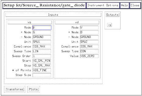
Preview / ig_vgs
This setup measures gate and drain voltage as a function of gate current. Four specific values of forward gate current are applied, with the drain current set to a constant value of 0.0A. The purpose of the setup is to use the gate current density of the device, and the gate width and length, to set the proper variable values for gate voltage.
This setup determines several gate voltages that will be used in later measurements, and sets their values in the variable table. These variables are VG_FWD_MAX, VG_FWD_MID, VG_FWD_MIN, and VG_FWD_IV.
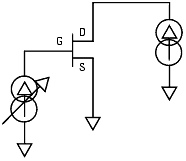
The input variables you set in the following procedure will configure the FET as shown in the following figure.
Figure 109 FET Bias Configuration for ig_vgs Measurement
|
|
To define the DC Source/Monitor instrument state, follow these instructions:
Initializing The Input Variable Values
The inputs control the measurement. The variables listed in the inputs use the numerical values from the variable table. You define the actual numerical values in response to prompts from the software. You generally do not need to change the inputs, but they are illustrated and explained for your information.
The values you use will be dependent on your knowledge of your device under test. As you observe the results of the preview measurements, you can change the variable table values until you are satisfied with the measured results.
| 1 |
If you have not already connected the device, do so now. Observe antistatic precautions. |
|
Note
|
|
|
|
|
Remove any high-intensity light sources such as microscope light before taking a measurement. One easy method of blocking light is to place an opaque plastic box on the fixture directly above the device.
|
|
| 2 |
Select Preview > ig_vgs. |
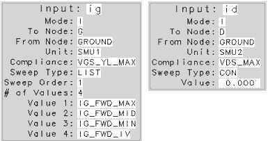
- Notice the inputs ig and id. These are used by the software to control the measurement. Note that Mode is set to I to provide a current to both ig and id inputs.
Figure 110 Preview / ig_vgs inputs
|
|
- The Unit names must conform to the names you set in the hardware window (see Getting Started in IC-CAP). They must also correspond with the actual plug-in SMU connections from the DC source/monitor. SMU1 is the gate supply and SMU2 is the drain supply. Since the source is grounded, only the gate and drain inputs need to be set.
- Compliance values limit SMU output voltage or current and prevent damage to the device under test, as well as to the SMUs, bias networks, and probes if used. With a current input, compliance refers to voltage. In the model variable table, set the Value of VGS_YL_MAX to a low value that will protect the device from overdrive on the gate. A value of 0.6V will work for nearly all devices, though occasionally it may need to be set to 0.7V or higher. Be sure to use a value within the resolution settability limits of the DC source/monitor.
| 3 |
In the model variable table, set the value of VDS_MAX to the largest safe Vds value for all Vgs values. Be aware of the power dissipation limits of your device at high Ids levels, to prevent damage to the device. |
- The Sweep Type for ig is set to List to allow four specific different gate current inputs. In list sweep mode, it is possible to specify up to 15 different bias inputs for the measurement. This measurement requires inputs of IG_FWD_MAX, IG_FWD_MID, IG_FWD_MIN, and IG_FWD_IV.
| 4 |
In the variable table, locate the values for IG_FWD_MAX, IG_FWD_MIN, and IG_FWD_IV. |
| 5 |
From the Extract/Optimize folder, select the update_ranges transform and click Execute. The transform will check for data and then update the appropriate variables. |
| 6 |
The updated variable values will be listed in the Status window. |
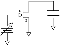
Preview / id_vgs_at_vdso
This setup measures drain current as a function of swept gate voltage, with drain voltage set to a constant bias value equal to Vdso. The gate voltage is swept across the operating range from minimum to maximum. The measurement covers all regions of device operation from subthreshold through threshold and high current regions.
Vdso is an important operating characteristic for most GaAs FETs. The model's IV equations simplify greatly at Vdso. Setting Vdso appropriately helps to ensure that the rest of the IV and the dispersion parameters will extract efficiently.
This setup determines several gate and drain voltage and current variables, and sets their values in the variable table.
The input variables you set in the following procedure configure the FET as shown in the following figure.
Figure 111 FET Bias Configuration for id_vgs_at_vdso Measurement
|
|
To define the DC Source/Monitor instrument state, follow these instructions:
|
Note
|
|
|
|
|
Use the same settings as you did for the ig_vgs measurement, except set Integ Time to L (long) for maximum averaging for this measurement.
|
|
Then return to this chapter and continue.
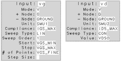
Initializing the Input Variable Values
| 1 |
Select Preview > id_vgs_at_vdso. |
- Notice the inputs vg and vd (see the following figure). Note that Mode is set to V to provide a voltage to both vg and vd inputs. With a voltage input, compliance refers to current.
Figure 112 Preview / id_vgs_at_vdso inputs
|
|
| 2 |
In the model variable table, set the Value of IGS_MAX no greater than the maximum allowable gate current for your device in amps. Be sure to use a value within the resolution settability limits of the DC source/monitor. Also note that the maximum output current of the Agilent 41421B medium-power SMU likely to be connected to the device gate is 0.100 amp. |
| 3 |
In the model variable table, set the Value of IDS_MAX lower than the maximum current for your device. The maximum output current of the Agilent 41420A high-power SMU likely to be connected to the device drain is 1.0 amp. |
| |
• |
In this model, the compliance for vg is always IGS_MAX and the compliance for vd is always IDS_MAX. |
| |
• |
The Sweep Type for vg is set to LIN to provide a linear voltage sweep from start to stop gate voltage values. The Sweep Type for vd is set to CON for a constant drain voltage value equal to Vdso. |
| 4 |
Set VGS_MAX to the highest (most positive) Vgs value where the device can be operated quiescently at VDS_MAX. (VDS_MAX is the largest safe Vds value for all Vgs values.) |
| 5 |
Set VGS_FINE to a fairly large number of points, sufficient to display the detail of the measurement across the trace. Typically, 101 points is an adequate number. Note that voltage steps in fractional mV increments do not work. |
| 6 |
From the Extract/Optimize folder, select the initialize transform and click Execute. The plots will be displayed, and screen prompts will ask you to input values for other variables needed in this measurement. Use values appropriate for your device. |
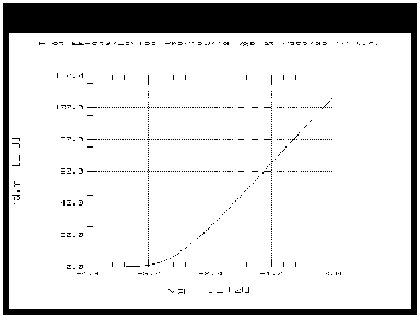
VDSO is one of the most important operating characteristics set in the model. Usually a transistor's static IV curves will peak up a little just after the device enters the saturation region. The value of Vds at this peak is a perfect value for Vdso. If the device shows no hump in the IV curves at about Vds=3.0V, select a Vdso value approximately 1V above the knee of the Vgs=0 curve. Vdso=3.0V is a good default and will nearly always work. It is important that Ids is at its quiescently measured maximum at this point. Device manufacturers often specify Idss at a value of Vds that is ideal as a setting for Vdso.
When you have responded to all the prompts, the transform measures the device and updates the plots. It sets appropriate numerical values for the relevant variables, and lists them in the model variable table and the Status window. Preliminary values for some of the model parameters will also be listed.
Figure 113 Example dc_iv Plot in the id_vgs_at_vdso Setup
|
|
The dc_iv plotted data should resemble the previous figure in shape, though the values will be specific to your device. It is most important to include data points in the subthreshold region. Note that as Vds becomes more positive the device threshold will tend to become more negative. If the data indicates the device is not operating in the correct range, you will need to redo the initialization and change the input variable values you set, particularly the VGS_MIN and/or VGS_MAX values.
| • |
If the measured data looks wrong for your device, check the probe contacts, the bias connections, and the measuring instruments. Make sure the device is oriented properly, with the right ports connected to the right terminals. If none of these resolves the problem, the device may be defective. |
| • |
If you want to save the measured data for later comparison with data predicted by the extracted model, choose File > Save As. Enter an appropriate filename (for example id_vgs_at_vdso), and click OK. |
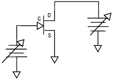
Preview / id_vds_vgs
This setup measures drain current with respect to drain voltage, at several values of gate voltage. The drain voltage is swept from 0V to the upper limit of its operating range. The measurement covers the overall region of device operation, and plots the characteristic IV curves vs. Vds.
The input variable values you set will configure the FET as shown in the following figure.
Figure 114 FET Bias Configuration for id_vds_vgs Measurement
|
|
Defining the DC Source/Monitor Instrument State
The instrument states need to be set independently for each setup. Use the same settings as you did for the id_vgs_at_vdso setup, except that you can set Integ Time to M (medium) to allow a faster measurement time: this measurement does not require maximum averaging.
Follow the steps described in the appropriate chapter shown next:
Then return to this chapter and continue.
Initializing the Input Variable Values
| 1 |
Select Preview > id_vds_vgs setup and observe the inputs vg and vd (see the following figure). |
Figure 115 Inputs for id_vds_vgs Measurement
|
|
| |
• |
Notice that for this measurement, both vg and vd are set with a Sweep Type of LIN to provide a linear sweep from minimum to maximum values. |
| |
• |
Note that the Sweep Order for vd is set to 1, and for vg is set to 2. |
| |
• |
The Start and Stop values for vg are set to VGS_MIN and VGS_MAX as in the previous measurement. However, # of Points is now set to VGS_COARSE. This represents the number of separate measurement traces that will be made of Id at evenly-stepped Vgs values. In the variable table, set the VGS_COARSE value to a fairly low number, between 5 and 15, so that the separate traces will be distinguishable. Remember that fractional mV step values will not work. |
| 2 |
For VDS_COARSE, set a number sufficient to display the measurement clearly across the trace but without the need for detail: an arbitrarily large number of data points does not increase model accuracy. A VDS_COARSE value between 5 and 15 will provide enough detail without unduly slowing the measurement. |
| 3 |
From the Plots folder, select the dc_iv plot and click Display Plot. A plot of the device characteristic curves will be displayed. |
| 4 |
Set VDS_MIN to the smallest value you will use for Vds. This is usually 0.0V, but may be a negative value. |
| 5 |
Set VDS_MAX to a value in saturation well above Vdso. This should be the largest safe Vds value for all Vgs values. Be aware of the power dissipation limits of your device at high Ids levels, to prevent damage to the device: Pdiss_MAX must not exceed VDS_MAX*IDS_MAX. |
- When you have input all the necessary values, click Measure. This measures the device and updates the plot. Review the plot and if needed change the necessary variables and re-measure.
Figure 116 Example Measured ids_vds_vgs Device Preview Data
|

|
- The plotted data should resemble the previous figure. If it does not, you may need to change the VDS and/or VGS variables. Continue until you have an appropriately nominal set of characteristic IV curves displayed, showing good coverage of the Vds and Vgs features.
| 6 |
Optionally, to save the measured data, choose File > Save As. Enter an appropriate filename and press Enter or click OK. |
The Source_Resistance DUT
There are many different approaches to the measurement and extraction of the common lead resistance in junction FET devices. Perhaps the most common is the "end resistance" measurement method where the unbiased drain terminal is used as a voltage probe to measure the voltage at the top end of Rs while a substantial current is forced into the gate. While that method is fairly good, it includes inaccuracy due to channel resistance effects. The method presented here overcomes the problem by correcting for the effect of the open channel resistance (see End Resistance Technique).
Modified End Resistance Measurement Technique
The Yang and Long method computes the value of Rs from the change in Vgs due to the application of two drain currents, which are 50 to 100 times greater than Ig. The two drain currents are chosen to be within the drain's linear IV region (Vds < 0.25 volts).
The data for the computation of Rs is taken by sweeping Ig over a range that results in measured Vgs values in the range of 0.300V to 0.600V. Two separate Ig sweeps are made, with current forced at the drain terminal at two levels. The smaller of the two Id currents is chosen to be within 10% of the larger.
The current values needed by this method are highly dependent on the voltage limits specified. The voltage limits, however, are nearly universal and will work with nearly any device. The process thus requires Preview to set the voltages, and then uses the voltage data to provide the needed current ranges.
The authors provide derivations for the shift in Vgs that depend only on the gate diode's active resistance and Rs. The form of these expressions cannot be reduced to Rs=xxx, so the measured and computed delta Vgs values are optimized until a suitable Rs is found.
In order for this method to work, the gate diode characteristics Is and N must first be known. These are characterized in the gate_diode measurement. Thus three setups are required for this technique: the Yang_Long_Preview, the gate_diode, and the Yang_Long_Method.
Source_Resistance / Yang_Long_Preview
This setup measures both Ig and Id as a function of Vg, and displays the results on a log scale. The setup is used to ensure that the current input values chosen fall within the limits prescribed in the original paper by Yang and Long.
In this setup the values for several Yang_Long method variables will be determined and set in the model variable table.
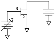
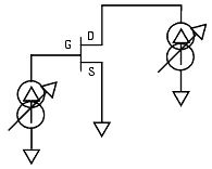
The input variables configure the FET as shown in the following figure.
Figure 117 FET Bias Configuration for Yang_Long_Preview Measurement
|

|
Defining the DC Source/Monitor Instrument State
Follow the steps described in the appropriate chapter shown next:
Use the same settings as you did for the device preview measurements, except set Integ Time to L. Then return to this chapter and continue.
Initializing the Input Variable Values
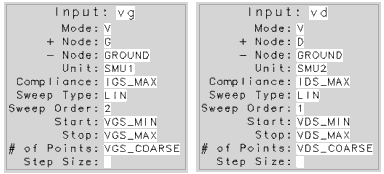
| 1 |
Select Source_Resistance > Yang_Long_Preview. and observe the inputs vg and vd (see the following figure). |
Figure 118 Inputs for Yang_Long_Preview Measurement
|
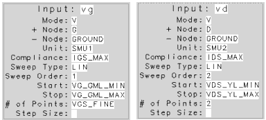
|
| |
• |
Both the vg and vd Sweep Type are set to LIN for a linear sweep from start to stop values. |
| |
• |
The vg # of Points is set to VGS_FINE to allow clear and accurate definition across the trace. |
| |
• |
The vd # of Points is set to 2 to provide Vd measurements at two closely spaced values. |
| 2 |
Select Extract/Optimize folder, select the initialize transform and click Execute. The transform selects the appropriate current values for the device under test and saves them in the variable table. |
- The VG_GML values should be set to voltages that comply with the methods defined by Yang and Long. Usually the defaults (0.3V for VG_GML_MIN and 0.6V for VG_GML_MAX) are adequate and you will probably not need to change them.
- The Rs extraction is done in the linear region of transistor operation. Therefore both VDS_YL_MIN and VDS_YL_MAX are values in the linear region of Vds, at values less than 0.25V. Generally, these Vds default values never need to be changed except in the case of a device with a very sharp knee.
| 3 |
Select the log10ig_id_by_vg plot and Display Plot. The plot should resemble the following figure, with measured traces for both Ig and Id, plotted on a log scale. Sometimes the top end of the measured range may show some resistive effects: this will be windowed out in the extraction procedure later. |
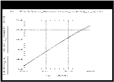
Figure 119 Example Yang_Long_Preview log10ig_id_by_vg Plot
|
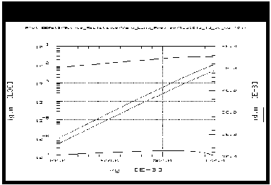
|
- The data on this plot is used to select current values to be used in the Yang_Long_Method setup. You will use the data to select the minimum and maximum values for IGS_YL and IDS_YL, which are used in the extraction of Rs.
| 4 |
Using the measured Ids traces, select lower and upper values for Ids that are within ten percent of each other, somewhere in the middle of the two traces. Select round numbers that are within the settability limits of the DC source/monitor. Enter your chosen values in response to the prompts for IDS_YL_MIN and IDS_YL_MAX. (The default value for IDS_YL_MIN is 0.058 amp, and for IDS_YL_MAX is 0.060 amp.) |
| 5 |
To select the values for Igs, pick values in the region of Igs where the trace is linear. Choose two values that are 50 to 100 times smaller than the Ids values you have chosen. Enter your chosen values in response to the prompts for IGS_YL_MIN and IGS_YL_MAX. (The default value for IGS_YL_MIN is 0.5E-4, and for IGS_YL_MAX is 0.5E-5.) |
- When you have input all the necessary values, the transform sets numerical values for the relevant variables, and lists them in the model variable table and the UNIX standard output window.
| 6 |
To save the plotted data, choose File > Save As. |
Source_Resistance / gate_diode
This setup measures swept gate current as a function of gate voltage, with Vds constant at zero, and displays the results on a log scale. This will be used for characterization of the gate diode forward conduction parameters Is and N. The dynamic resistance attributable to the gate diode formed by the Schottky contact is important to the extraction of all contact resistances.
The FET configuration is illustrated in the following figure.
Figure 120 FET Bias Configuration for gate_diode Measurement
|
|
Defining the DC Source/Monitor Instrument State
Follow the steps described in the appropriate chapter shown next:
Use the same settings as you did for the device preview measurements. Then return to this chapter and continue.
Setting the Input Variables
| 1 |
From the DUT/Setup panel select the gate_diode setup and observe the vg and vd inputs. The following figure illustrates the inputs used in this measurement. |
Figure 121 Inputs for gate_diode Measurement
|
|
| |
• |
The vg inputs are the same as in the Yang_Long_Preview measurement, with the gate voltage set to sweep over the voltage range from VG_GML_MIN to VG_GML_MAX. |
| |
• |
vd is set to a CONstant voltage of 0.0. |
Measuring and Plotting
| 1 |
Select the log_ig_vg plot, and Display Plot. then click Measure. The plot should resemble the following figure, with Ig plotted on a log scale vs. Vg. |
| 2 |
The transform to compute the value of Ig will be performed in the extraction part of the procedures. |
Figure 122 Example gate_diode log_ig_vg Plot
|
|
| 3 |
Optionally, to save the plotted data, choose File > Save As. |
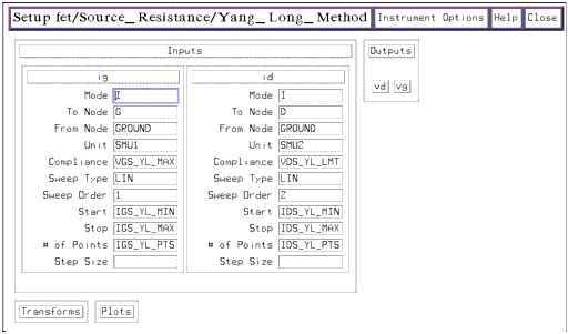
Source_Resistance / Yang_Long_Method
This procedure uses Ids and Igs values derived from the results of the Yang_Long_Preview measurement. The setup drives two different relatively small amounts of drain current into the device. It sweeps Igs values that are 50 to 100 times smaller than Ids, to give measured Vgs values that differ slightly: the difference is due to the common lead resistance.
Device Configuration: The input variables configure the FET as shown in the following figure.
Figure 123 FET Bias Configuration for Yang_Long_Method Measurement
|
|
Defining the DC Source/Monitor Instrument State
Follow the steps described in the appropriate chapter shown next:
Use the same settings as you did for the device preview measurements. Then return to this chapter and continue.
The Input Variables
| 1 |
To view the input variables for this measurement, from the DUT/Setup panel, select the Yang_Long_Method setup and observe the vg and vd inputs. The following figure illustrates the inputs used in this measurement. |
Figure 124 Inputs for Yang_Long_Method Measurement
|
|
| |
• |
Note that for this current-controlled measurement, the Compliances are voltage values. |
| |
• |
The ig Sweep Type is set to LIN for a linear gate current sweep from IGS_YL_MIN to IGS_YL_MAX. These are the extremely small positive voltage values you selected from the measured Yang_Long_Preview data. The IGS_YL_PTS default value of 11 is adequate. |
| |
• |
The id Sweep Type is set to LIN for a linear sweep measured at the IDS_YL_MIN and IDS_YL_MAX values you selected from the measured Yang_Long_Preview data. The IDS_YL_PTS value is always set to 2 for two swept traces. |
Measuring and Plotting
| 1 |
From the Plots folder (for the Yang_Long_Method setup), select the delta_m_s plot, and Display Plot, then click Measure. The plot should resemble the following figure. |
Figure 125 Example Yang_Long_Method delta_m_s Plot
|
|
| 2 |
Select the opt_rs transform and Execute. |
| 3 |
Optionally, to save the plotted data, choose File > Save As. |
Parasitics Measurements: The cold_fet and package DUTs
The extractions for intrinsic and extrinsic parasitics are performed on S-parameter data measured with a calibrated network analyzer. These measurements are made in the following setups:
The cold_fet/rg_rd setup
The Rg and Rd contact resistances are extracted from cold FET measurements made with the device strongly forward-biased in both the gate-drain and gate-source regions. The method is similar to the work described by Dambrine, Cappy, et al.
Successful extraction of certain extrinsic parasitic elements is dependent on forcing the active device under test to a bias condition where its linear equivalent circuit reduces to a very simple form. While the Curtice model uses the "cold FET" method (Vds=0.0V, Vgs=0.0V) to optimize the contact resistances and parasitic inductances of the bond wires, further simplification can be achieved by strongly forward biasing the gate-source and gate-drain regions of the FET. This procedure is based on this premise.
Under conditions of strong forward gate bias the intrinsic charge model of the FET is shunted by small resistances of the forward active diode in the gate and the fully open channel between the drain and source. Under these circumstances the reactive behavior of the device is attributable to the lead inductances of the device. Both the drain and gate resistances are separable if the value of Rs is known.
This setup is substantially the same as the work of Dambrine and Cappy, though it does not exactly track their work (see Contact Parasitic Resistance and Inductance Method). The FET is forward-biased at three to five points. The extrinsic elements are constant while the gate and channel characteristics change.
Device Configuration: The following figure illustrates the device configuration for this measurement. For S-parameter measurements, a DC-biased RF signal is applied to the device gate from the network analyzer system source via the bias networks.
Figure 126 FET Bias Configuration for rg_rd Measurement
|
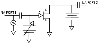
|
Defining the Instrument States
You will need to set the instrument states for both the DC source/monitor and the network analyzer.
For the DC source/monitor, use the same settings as you did for the device preview measurements. Calibrate the network analyzer. In the instrument options for the network analyzer, be sure to set the Cal Set No to the cal set or register where you save your calibration.
To define the DC Source/Monitor instrument state, follow these instructions:
You will use these instrument states in all the setups that make S-parameter measurements with the network analyzer. Then return to this chapter and continue.
Setting the Input Variables
| 1 |
Select the rg_rd setup to view the inputs and outputs. Notice The frequency input is set to LIN for a linear sweep over the calibrated network analyzer frequency range. |
| 2 |
Click the Model Variables tab and set FREQ_START, FREQ_STOP, and FREQ_POINTS to the start frequency, stop frequency, and number of frequency points you used for your network analyzer calibration. |
- Notice the input vg is set to sweep at three specific values that will heavily forward bias the gate diode.
- Notice the input vd is set to CON for a constant value of VDS_ZERO.
Measuring and Plotting
| 1 |
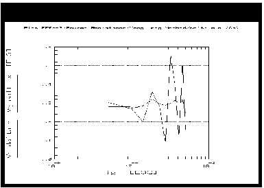
In the rg_rd setup select the im_z12 plot, and Display Plot. then click Measure. The plot should resemble the following figure. The data plotted is the imaginary part of the intrinsic Z12, derived from S12, which will be used in the extraction procedures to give preliminary values for the bond inductances, as well as the Rg and Rd values. |
Figure 127 Example im_z12 Plot in the rg_rd Setup
|
|
Package Parasitics: the package DUT
RF parameter extraction and large-signal model generation require the reduction of a large number of S-parameter sets into an equivalent circuit format. Although numerical optimization techniques have often been used for extracting these small-signal models, their problems with uniqueness and long execution times make them impractical here. Fast techniques for extracting complete small-signal models have been described previously but all require the additional RF characterization of the cold FET in order to extract parasitic inductance. This offers preliminary inductance values, but the values are not completely accurate since the model has not been derived solely from the data it is asked to model.
The method described here is derived from the work of Arnold and Golio et al (see Extraction of Package Parasitic and Intrinsic FET Equivalent Circuit Values). It requires only RF characterization at the device operating point and knowledge of the parasitic resistances. The technique has been successfully applied to GaAs FETs and HEMTs. After determining the parasitic resistances from DC measurements, the remaining elements are computed directly from a single set of measured S-parameters. The method is very fast, and its results provide an excellent match to measured S-parameters throughout the saturation region.
The package/Arnold_Golio setup
The package resistance and inductance parasitics are extracted from S-parameter data measured across Vgs with Vds at the nominal operating point. It is particularly important to make sure the nominal operating conditions are used for extractions of contact resistance and parasitic parameters, otherwise errors are caused by bias dependencies that are not modeled.
This setup measures S-parameters at values of Vgs from pinchoff to Idss at the nominal Vds operating bias point. This large range of Vgs values allows the largest intrinsic model variations possible. Large variations in the FET element values increase the impact of the static package parasitics, making them easier to extract in the later procedures. The accuracy of this measurement is very dependent on a good network analyzer calibration.
Device configuration:
Figure 128 FET Bias Configuration for Arnold_Golio Measurement
|
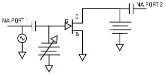
|
Defining the Instrument States
Use the same instrument state settings for this procedure as you did for the rg_rd measurement, for both the DC source/monitor and the network analyzer. The instrument states need to be set independently for each setup.
To define the DC Source/Monitor instrument state, follow these instructions:
Then return to this chapter and continue.
Setting the Input Variables
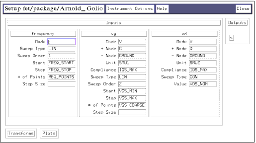
| 1 |
Select the Arnold_Golio setup and observe the inputs. The following figure illustrates the inputs used in this measurement. |
Figure 129 Inputs for Arnold_Golio Measurement
|
|
| |
• |
The frequency inputs are set the same as for the rg_rd measurement. |
| |
• |
The vg value of VGS_MIN (which you set in the device preview measurements) is a value that is more negative than the device pinchoff voltage at the nominal operating voltage of Vds. |
| |
• |
VGS_MAX (set in device preview) is the highest (most positive) Vgs value where the device can be operated quiescently at VDS_MAX. |
| |
• |
VGS_COARSE is a number of points between 5 and 15. |
| |
• |
Vd is set for a CONstant value of VDS_NOM, the nominal operating voltage of the device. VDS_NOM has not been used in any of the measurements so far, so you may need to set the value in the variable table. |
Measuring and Plotting
| 1 |
From the Arnold_Golio setup, open the Plots folder and Display Plots, then click Measure. |
| 2 |
Optionally, to save the plotted data, choose File > Save As. |
The dc_iv DUT
The setups in the dc_iv DUT are used to obtain data for extracting DC-IV parameters. The setups used for these measurements are:
The measurement procedures are straightforward, and in most cases are duplicates of measurements you have made in device preview or as part of the source resistance measurements. Therefore, in the majority of cases, you have already defined the measurement input values in the model variable table or in response to prompts, and will not need to modify the inputs. However, the inputs are illustrated and explained for clarification of how each measurement is made. You will need to define the instrument states in each setup.
To prevent possible bias oscillation, put the network analyzer in hold sweep mode.
dc_iv / ig_Is_N (Measuring)
This is the same measurement made in the gate_diode setup as part of the source resistance measurements. It measures swept gate current as a function of gate voltage with Vds constant at zero, and displays the results on a log scale.
Defining the DC Source/Monitor Instrument State
Follow the steps described in the appropriate chapter shown next:
Use the same settings as you did for the device preview measurements. Then return to this chapter and continue.
The Input Variables
| 1 |
From the DUT/Setup panel, select the ig_Is_N setup and observe the inputs, as illustrated in the following figure. |
Figure 130 Inputs for ig_Is_N Measurement
|
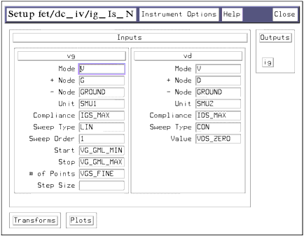
|
| |
• |
The gate voltage is set to sweep over the same Gummel range as in the gate_diode measurement. |
| |
• |
The drain voltage is set to VDS_ZERO. |
Measuring and Plotting
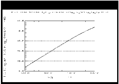
| 1 |
Select the log_ig_vg plot, and Display Plot and then click Measure. The plot should resemble the following figure, with Ig plotted on a log scale vs. Vg. |
Figure 131 Example log_ig_vg Plot in the ig_Is_N Setup
|
|
| 2 |
Optionally, to save the plotted data, choose File > Save As. |
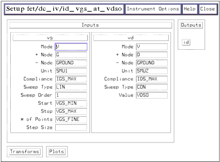
dc_iv / id_vgs_at_vdso (Measuring)
This is the same as the ids_vgs_at_vdso measurement you made as part of the device preview measurements. This measures all the values of Vg with Vds at a constant value of Vdso. It covers all regions of device operation from subthreshold up to the high current region.
Defining the DC Source/Monitor Instrument State
Follow the steps described in the appropriate chapter shown next:
Use the same settings as you did for the device preview measurements. Then return to this chapter and continue.
The Input Variables
| 1 |
From the dc_iv DUT, select the id_vgs_at_vdso setup and observe the inputs as illustrated in the following figure. |
Figure 132 Inputs for id_vgs_at_vdso Measurement
|
|
| |
• |
The gate voltage is set to sweep across the device operating range from minimum to maximum. |
| |
• |
The drain voltage is set to a constant value equal to Vdso, the point where the model equations simplify. |
Measuring and Plotting
| 1 |
Select the id_vg plot, and Display Plot. then click Measure. The plot should resemble the following figure with a single curve IV plot. |
Figure 133 Example id_vg Plot in the id_vgs_at_vdso Setup
|
|
| 2 |
Optionally, to save the plotted data, choose File > Save As. |
dc_iv / id_vgs (Measuring)
This procedure measures drain current with respect to drain voltage at several values of gate voltage. The drain voltage is swept from 0V to the upper limit of its operating range.
Defining the DC Source/Monitor Instrument State
Follow the steps described in the appropriate chapter shown next:
Use the same settings as you did for the device preview measurements. Then return to this chapter and continue.
The Input Variables
- Select the id_vgs setup and observe the inputs. The following figure illustrates the inputs for this measurement.
Figure 134 Inputs for id_vgs Measurement
|
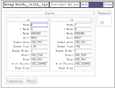
|
| |
• |
The gate voltage is set to sweep across the device operating range from minimum to maximum. |
| |
• |
The drain voltage is set to sweep from its minimum value to its maximum safe value. |
Measuring and Plotting
| 1 |
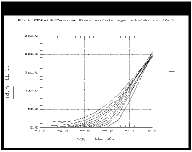
Select the id_vg plot, and Display Plot then click Measure. The plot should resemble the following figure. |
Figure 135 Example id_vg Plot in the id_vgs Setup
|
|
| 2 |
Optionally, to save the plotted data, choose File > Save As. |
dc_iv / id_vds (Measuring)
This is the same as the ids_vds_vgs measurement you made as part of the device preview measurements. The drain voltage is swept from 0V to the upper limit of its operating range. The measurement covers the overall region of device operation, and plots the characteristic IV curves vs. Vds. It uses the same inputs as the id_vgs measurement, except with the sweep order for vg and vd reversed.
Defining the DC Source/Monitor Instrument State
Follow the steps described in the appropriate chapter shown next:
Use the same settings as you did for the device preview measurements. Then return to this chapter and continue.
The Input Variables
| 1 |
Select the id_vds setup and observe the inputs, as illustrated in the following figure. |
Figure 136 Inputs for the id_vds Measurement
|
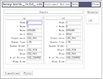
|
| |
• |
The gate and drain voltage values are set the same as for the id_vgs measurement. |
| |
• |
Note that the Sweep Order for vg is set to 2, and for vd is set to 1 to make the drain voltage the primary sweep. |
Measuring and Plotting
| 1 |
From the Plots folder select the id_vd plot, and Display Plot then click Measure. The plot should resemble the following figure, displaying the device characteristic curves. |
Figure 137 Example id_vd Plot in the id_vds Setup
|
|
| 2 |
Optionally, to save the plotted data, choose File > Save As. |
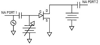
The AC_at_VDSO DUT
This DUT is used for making AC charge and dispersion parameter measurements. Two different S-parameter measurements are necessary for the extractions of the AC charge and dispersion parameters. The first measurement is performed with Vds set to a constant bias value of Vdso. The second has Vds actively biased across the device operating range. It is essential that the measurements be performed in the order listed, and that the extractions listed in the same DUT groupings with the measurement setups be performed from those corresponding setups. The extraction procedures later in the chapter will make clear which measurement setup is to be used for which extraction.
Make sure the network analyzer is in continuous sweep mode.
AC_at_VDSO / Meas_Spars
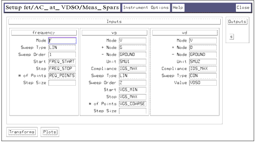
This setup measures S-parameters at values of Vgs from pinchoff to Vgs_max with Vds at Vdso, the point where the model equations simplify. The large range of Vgs values allows the largest intrinsic model variations possible, increasing the impact of the charge parameters and making them easier to extract. A good network analyzer calibration is important to the accuracy of this measurement and the subsequent charge parameter extractions.
Device Configuration: The following figure illustrates the device configuration for this measurement. A DC-biased RF signal is applied to the device gate from the network analyzer system source via the bias networks.
Figure 138 FET Bias Configuration for the First Meas_Spars Measurement
|
|
Defining the Instrument States
You need to set the instrument states for both the DC source/monitor and the network analyzer.
To define the DC Source/Monitor instrument state, follow these instructions:
Use the same instrument state settings for this procedure as you did for the rg_rd and Arnold_Golio measurements. Then return to this chapter and continue.
The Input Variables
- From the AC_at_VDSO DUT, select the Meas_Spars setup and observe the inputs. The following figure illustrates the inputs used in this measurement.
Figure 139 Inputs for the First Meas_Spars Measurement
|
|
| |
• |
The frequency inputs are set the same for all S-parameter measurements in this model, corresponding with the frequency settings of the network analyzer calibration. |
| |
• |
The gate voltage is set to sweep across the device operating range from minimum to maximum. |
| |
• |
The vg # of Points is set to VGS_COARSE. This ensures that the data taken is the least that will yield good measurement results with S-parameter plots that are understandable. Using too many measurement points causes the extractions to be very time-consuming and the plots to be confusing. |
| |
• |
The drain voltage is set to a CONstant value equal to Vdso, the point where the model equations simplify. |
Measuring and Plotting
| 1 |
With the Meas_Spars setup selected, Display Plots then click Measure. |
| 2 |
Optionally, to save the plotted data, choose File > Save As. |
About the Other Setups in the AC_at_VDSO DUT
Note that no measurements are performed in the other setups in this DUT. These setups will be used later, in the extraction procedures, based on the data measured in this first Meas_Spars setup. However, it is important that the DC input variables for vg and vd be set exactly the same as in the first Meas_Spars setup, with one exception. The exception is that the vg Sweep Order is set to 1 instead of 2, because there is no frequency sweep.
AC_all / Meas_Spars
This setup measures S-parameters at values of Vgs from pinchoff to Vgs_max and values of Vds swept across the device operating range. Again, a good network analyzer calibration is essential: if the calibration is incorrect or has drifted, the modeled data will be impossible to fit to the measured data.
Device Configuration:
Figure 140 FET Bias Configuration for the Second Meas_Spars Measurement
|
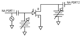
|
Defining the Instrument States
To define the DC Source/Monitor instrument state, follow these instructions:
Use the same DC source/monitor and network analyzer settings as you did for the first Meas_Spars and the other S-parameter measurements. Then return to this chapter and continue.
The Input Variables
- From the AC_all DUT, select the Meas_Spars setup and observe the inputs. The following figure illustrates the inputs used in this measurement.
Figure 141 Inputs for the Second Meas_Spars Measurement
|
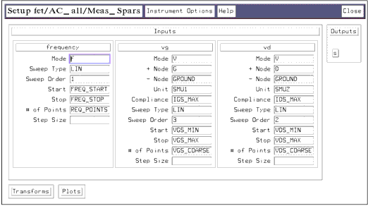
|
| |
• |
The frequency inputs are set the same as for the other S-parameter measurements. |
| |
• |
The gate voltage is set to sweep across the device operating range from minimum to maximum. |
| |
• |
The drain voltage is set to sweep from its minimum value to its maximum safe value. |
| |
• |
The # of POINTS for both vg and vd is set to COARSE to allow good measurement results without excessive data-taking. |
Measuring and Plotting
| 1 |
With the Meas_Spars setup selected, Display Plots then click Measure. |
| 2 |
Optionally, to save the plotted data, choose File > Save As. |
About the Other Setups in the AC_all DUT
Note that no measurements are performed in the other setups in this DUT. They will be used later, in the extraction procedures, based on the data measured in the second Meas_Spars setup. However, it is important that the DC input variables for vg and vd be set exactly the same as in the second Meas_Spars setup, with one exception. The exception is the Sweep Order, which is set to 1 for vg and 2 for vd, because there is no primary frequency sweep.
Storing the Measured Data
This procedure stores the data you measured for this particular device. You can then use the data to perform the extractions, to compare the simulated data with the measured data, and as a measurement record for comparison with other devices.
If you will be measuring large numbers of devices, it is worthwhile to organize your directory structure according to device type, geometry, and batch or wafer.
| 1 |
Decide where in your directory structure you intend to store this data file. |
| 2 |
From the IC-CAP/Main window select Model, then select File > Save As from the pulldown menu. A dialog box is displayed. |
| 3 |
Choose a filename that will clearly identify the measured device and the type of information stored, such as fet2_meas_12aug95. Type the directory path and the filename into the dialog box. |
| 4 |
Click OK or press Enter to store the data and close the dialog box. |
| 5 |
When you want to use this data for an extraction at some future date, remember to change directories in IC-CAP by selecting Windows > Main Window and File > Change Directory... (See Accessing Data from a Previous Measurement.) |
This concludes the measurement procedures. The extraction procedures follow.
Parameter Extractions
Once the measurements have been performed and a complete set of data collected for a particular device, the extraction can proceed. If you saved the measured data, you can perform an extraction at any later time. The Xtract macro can be used for an unattended extraction, or each extraction step can be processed individually to allow complete process control. The procedures in the following pages explain how to extract the parameters individually.
Displaying the Parameters Table
If the Parameters table is not already displayed on the screen, select Model Parameters from the Model window, and select Detach.... Move the Parameters table to a convenient corner of the screen: you will be using it throughout the extractions.
Extracting the Source Parasitic Resistance Rs
The Yang and Long method computes the value of Rs from the change in Vgs due to the application of two drain currents, which are 50 to 100 times greater than Ig. The two drain currents are within the drain's linear IV region (Vds < 0.25 volts). The smaller of the two Id currents is within 10% of the larger. The values were set in the source resistance measurement procedures.
The authors Yang and Long provide derivations for the shift in Vgs that depend only on the gate diode's active resistance and Rs. The form of these expressions cannot be reduced to Rs=xxx, so the measured and computed delta Vgs values are optimized until a suitable Rs is found.
In order for this method to work, the gate diode characteristics Is and N must first be known. These are extracted from the data measured in the gate_diode setup. Thus two setups are required for this extraction: the gate_diode and the Yang_Long_Method setups.
Extracting Is and N
| 1 |
In the Parameters table, locate the values for EEFET3.rs, Is, and n. |
| 2 |
From the DUT/Setup panel, select the gate_diode setup, and select the Plots folder. |
| 3 |
From the Plots folder select log_ig_vg, and Display Plot. The plot shows Ig plotted on a log scale vs Vg. |
| 4 |
From the Extract/Optimize folder, select the opt_is_n transform. |
| 5 |
Click the Parameters tab to view the lower and upper optimization limits for EEFET3.Is and .n. |
| 6 |
Click the Inputs tab to view the upper and lower bounds for Vgs that should limit the optimization range to the linear portion of the IV curve. If for some reason these limits are not sufficient, use the next step to establish more restrictive limits. |
| 7 |
Click the Options tab to view the X_LOW, X_HIGH, Y_LOW, and Y_HIGH functions. These are optimization limits you can set from the data plot to select a portion of the trace for the optimization. The gate diode parameters should be optimized over only the linear portion of the trace, so use the X-low/X-high function as follows: |
| |
• |
Select setup gate_diode, then select Setup Variables folder. A variable table will appear, with current values for X-LOW and X-HIGH. |
| |
• |
From the plotted data choose a linear portion of the trace, along the constant slope. |
Figure 142 Log Plot of Ig vs. Vg, with X-Low/X-High Values Selected
|
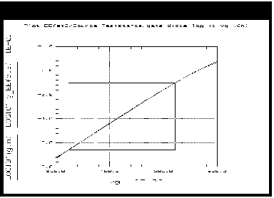
|
| |
• |
Put the mouse pointer at the low end of the chosen portion and click left, then put the pointer at the high end and click left, to make a box on the trace, as shown in the previous figure. |
| |
• |
From the plot select Options > Copy to Variables. This changes the X_LOW and X_HIGH values to the lower and upper limits you selected on the trace. |
| 8 |
Click Execute. The transform optimizes the plotted data, using the linear portion of the trace you defined with X-low/X-high, and enters the optimized values for Is and n in the Parameters table. |
Optimizing Rs
Driving two different relatively small amounts of drain current into a FET and then making swept Vgs measurements vs. Igs gives two sets of measured Vgs values that differ slightly. The difference is due to the common lead resistance. Measured and simulated delta_Vgs values are optimized in this procedure to yield a reasonable value of the common lead resistance Rs.
|
Note
|
|
|
|
|
This extraction generally uses current values within the limits prescribed in Yang and Long's original paper. (These are values you set in the Yang_Long_Preview measurement procedure.) If you chose values outside these limits, warning messages in the extraction phase will alert you to that fact. However, the warnings will not prevent the computations from completion, as you may have a valid reason not to use the specified limits: in this case, ignore the warning messages and use the computed values.
|
|
| 1 |
Select the Yang_Long_Method setup, and Display Plots. |
Figure 143 Example Yang_Long_Method by_vgs Plot
|
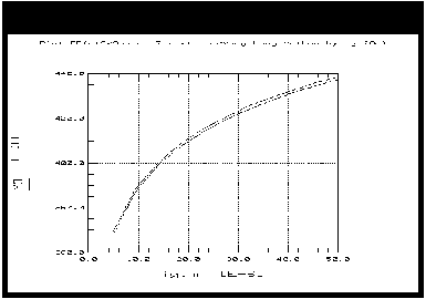
|
| 2 |
From the Extract/Optimize folder, select opt_rs, and Execute. Observe the plots as the traces converge. The by_vgs plot shows the difference between the measured and simulated data. |
- The opt_rs transform also calls the Vg_delta_m and Vg_delta_s transforms, so you need not perform them separately. The transforms optimize the measured and simulated Vgs shifts for the most accurate source resistance extraction.
Figure 144 The Computed Shift in Measured and Simulated Vgs Values
|
|
- The difference in measured and simulated Vgs values is used for the calculation of Rs. The previous figure illustrates the results of the optimization. The difference in Vgs values is caused by the common (source) lead resistance. Although the traces appear very different, note that the scale is very small and the values result in differences of fractions of an ohm.
Extracting the Contact Resistances Rd and Rg
This extraction uses a device setup with the gate-source and gate-drain junctions of the FET strongly forward biased. Under conditions of strong forward gate bias the intrinsic charge model of the FET is shunted by small resistances of the forward active diode in the gate and the fully open channel between the drain and source. Under these circumstances the reactive behavior of the device is attributable to the lead inductances. Both the drain and gate resistances are separable if the value of Rs is known.
The FET is forward-biased at three to five points. The extrinsic elements are constant while the gate and channel characteristics change. In this extraction the extrinsic elements are optimized while the intrinsic device resistances are allowed to shift. The values of the extrinsic inductance elements are only initial values that will be refined in a later procedure.
This extraction is based on the S-parameter data you measured in the rg_rd setup. A transform in this extraction computes and saves a table of linear equivalent circuit parameters based on the measured S-parameters. It calculates the contact resistance parameters directly from the measured data, and allows you to compare the linear model extracted to the measured S-parameters.
| 1 |
In the Parameters table, locate the values for EEFET3.rg and rd. |
| 2 |
From the DUT/Setup panel, select the rg_rd setup. |
| 3 |
From the Plots folder, select the im_Z12 plot, and Display Plot. The data plotted is the imaginary part of the intrinsic Z12, derived from S12. |
| 4 |
From the Extract/Optimize folder, select the auto_extr transform and Execute. This computes the values for the parasitic resistances Rg and Rd. It also calculates initial values for the parasitic inductances Lg, Ld, and Ls, which will be refined in the next procedure. The pad capacitances are defaulted to 0.0 for this procedure, and will be extracted later. |
- The calculated values for EEFET3.rg and rd will be entered in the Parameters table. Values for Rs, Rd, and Rg, as well as Ls, Lg, and Ld, will be displayed in the UNIX standard output window. An example of the calculated Z-parameter data is illustrated in the following figure.
Figure 145 Example im_Z12 Data in the rg_rd Setup
|
|
Extracting the Package Parasitics
This extraction is based on the S-parameter data you measured in the Arnold_Golio setup (S-parameters at values of Vgs from pinchoff to Idss at the nominal Vds operating bias point). As the device goes through this wide range of measurement variations the package parasitic inductances remain constant, allowing them to be readily extracted.
A transform in this extraction computes and saves a set of linear equivalent circuit parameters based on the measured S-parameters. A set of modeled S-parameters are simulated based on the linear equivalent circuit. Any differences between the simulated and measured S-parameters are due to the package parasitics or to defects in the network analyzer calibration. (This is why a good network analyzer calibration is essential for success in this extraction.) A second transform optimizes the measured and simulated S-parameter data to extract the package parasitic inductances.
| 1 |
In the Parameters table, locate the values for lg.l, ld.l and ls.l. |
| 2 |
From the DUT/Setup panel, select the Arnold_Golio setup, and Display Plots. |
| 3 |
From the Extract/Optimize folder, select mdl, and Execute. This computes a set of linear equivalent circuit parameters based on the measured S-parameters, and uses them to simulate a set of modeled S-parameters. |
| 4 |
Select the transform opt_pkg, and Execute. This calculates the values for the package parasitic inductances. |
- You will see the traces converge on the plots, and the new calculated values for lg.l, ld.l, and ls.l will be entered in the Parameters table. Note that these are final values for the initial inductances calculated in the last procedure.
| 5 |
Optionally, you can change the optimization limits. Select Arnold_Golio setup, and Setup Variables. Modify values in the table as required. |
Extracting DC-IV Parameters
The DC-IV extractions start with preliminary estimates of some parameters and begin to establish firm values for some others. Four measurement setups and their measured data are used. The fourth and last DC extraction finalizes the initial values determined in the three previous setups.
Note that the thermal factor Peff has a major impact on the performance of nearly all model parameters. Therefore the initial value for Peff is set so high that it has no impact on model performance.
dc_iv / ig_Is_N (Extracting)
This procedure uses measured gate current data to extract final values for the gate diode characteristics Is and N. (Initial values were found in the source resistance extraction using the gate_diode setup.)
| 1 |
Locate the value for EEFET3.peff in the Parameters table. Make sure the Value is set to a high number such as 100, high enough that it will have no effect on model performance. |
| 2 |
Locate the values for EEFET3.Is and n. |
| 3 |
From the DUT/Setup panel, select the ig_Is_N setup. |
| 4 |
From the Plots folder, select log_ig_vg plot, and Display Plot. The graph shows Ig plotted on a log scale vs. Vg. |
- The parameters should be optimized over only the linear portion of the trace. The input table contains upper and lower bounds for Vgs that should limit the optimization range to the linear portion of the IV curves. If for some reason these limits are not sufficient, use the X-low/X-high function to define the limits for a window of the linear trace.
| 5 |
From the Extract/Optimize folder select opt_is_n, and Execute. The transform optimizes the plotted data, using the linear portion of the trace you defined with X-low/X-high, and enters the optimized values for Is and n in the Parameters table. |
dc_iv / id_vgs_at_vdso (Extracting)
This procedure uses measured Ids data with Vg swept across the device operating range and Vd set to a constant value of Vdso. Thus it covers all regions of device operation from subthreshold up to the high current region, and makes use of the fact that the model equations simplify at Vdso.
This data is used to set the value of Vto and to plot a curve for Gm. From these values the procedure extracts initial values for Vgo and Vdelt, as well as several other FET and HEMT parameters.
| 1 |
Leave EEFET3.peff set to a high value. |
| 2 |
Locate the values for EEFET3.vt and EEFET3.vdelt. |
| 3 |
From the dc-iv DUT, select the id_vgs_at_vdso setup, and Display Plots. |
| 4 |
From the Extract/Optimize folder, select the initialize transform and Execute. This sets up the software to extract the device-specific parameters. |
| 5 |
Select opt_vto_fet3 for a FET, or opt_vto_hemt1 for a HEMT, and Execute. The transform optimizes the plotted data, and enters the optimized values into the Parameters table. |
dc_iv / id_vgs (Extracting)
This procedure is used to calculate an initial value for gamma, the parameter that controls the amount Vto shifts with increasing Vds. The final value for gamma will be refined in the last DC extraction.
The control range set for the data optimization is very important in this procedure.
| 1 |
Leave EEFET3.peff set to a high value. |
| 2 |
Locate the value for EEFET3.gamma. |
| 3 |
From the DUT/Setup panel select the id_vgs setup. |
| 4 |
From the Plots folder, select id_vg plot, and Display Plot. |
| 5 |
In the Model window select Setup Variables. Note the default values for Y_LOW and Y_HIGH. This control range for the data optimized is important: low values of Ids must be used. Ids values have to be windowed so that only the first 5% to 10% of the Ids data is used, usually between 0.0 and a few milliamps for each trace. The X values should be left at 0 to ensure that all the X-axis data is used in the optimization. |
| 6 |
From Extract/Optimize folder, select opt_gamma and Execute. You will see the low end of the traces converge on the plot, and the new calculated value for gamma will be entered in the Parameters table. The following figure shows an example of the initial optimized gamma data. |
Figure 146 Example Initial Optimized Gamma Data in the id_vgs Setup
|
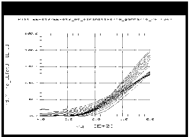
|
- Since this is an initial extraction step, the model fit is not ideal. Certain effects will be better modeled in subsequent stages.
dc_ic / id_vds (Extracting)
This procedure extracts final values for parameters initially extracted in the DC-IV extraction procedures. In addition to Vdelt and Gamma, this procedure extracts the parameters Kappa, Vsat, and Peff.
| 1 |
Locate the values for EEFET3.vdelt, vsat, and vgo in the Parameters table. |
| 2 |
From the DUT/Setup panel, select the id_vds setup and display the id_vd plot. |
| 3 |
From the Extract/Optimize folder, select opt_iv_fet3 or opt_iv_hemt1, and Execute. The transform optimizes the plotted data, and enters the optimized parameter values in the Parameters table. |
- Use the X-low/X-high function if desired, to select only a portion of the data for the optimization. This is appropriate if any of the plotted data looks anomalous.
| 4 |
Locate the optimized values for EEFET3.gamma, kappa, and peff in the Parameters table. You will notice that the value for EEFET3.peff has changed significantly. The following figure shows an example of the final optimized DC-IV curves. |
Figure 147 Example Plot of Final Optimized DC-IV Data
|
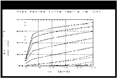
|
- If you decide to rework the DC-IV extraction phase, make sure to reset EEFET3.peff to a high value such as 100.
Extracting Charge and Dispersion Parameters
Charge parameters are divided into two groups:
| • |
The gate charge parameter extraction is based on the S-parameter data measured at Vdso in AC_at_VDSO/ Meas_Spars. |
| • |
The output charge and dispersion parameter extractions are based on the S-parameter data measured with active DC bias in AC_all/Meas_Spars. |
It is important that the individual extractions are based on the correct set of S-parameter data: the data from the same DUTs in which the extractions are grouped. If the setups are mixed within DUTs or performed in the wrong sequence, the results will be wrong.
A transform in each procedure computes a set of linear equivalent circuit parameters based on the measured S-parameter data. The actual model parameters are extracted from this linear equivalent circuit data.
The dispersion parameters are grouped here together with the charge parameters because they also are extracted from the S-parameter data measured with active bias.
Extracting Gate Charge Parameters
This procedure uses the S-parameter data you measured in the first Meas_Spars procedure. Since the model equations simplify at Vdso, the charge parameters C11o and C11th, Vinfl, and Deltgs can most accurately be extracted with Vds set to a constant value of Vdso. These are initial values for C11o and C11th.
Extracting the Linear Equivalent Circuit
| 1 |
From the AC_at_VDSO DUT, select the Meas_Spars setup and Display Plots. |
| 2 |
From Extract/Optimize folder, select mdl and Execute. This computes and saves a set of linear equivalent circuit parameters based on the measured S-parameters. Observe the changes in the plots. |
Extracting C11 Capacitance with C11_vgs
This procedure extracts the C11 capacitance looking into the gate terminal.
| 1 |
Locate the values for EEFET3.c11o, c11th, vinfl, and deltgs (near the bottom of the table). |
| 2 |
Select the setup C11_vgs. |
| 3 |
From the Plots folder, select the C11 plot, and Display Plot. |
| 4 |
From the Extract/Optimize folder, select the initialize transform, and Execute to establish initial values. |
| 5 |
Select the transform opt_to_C11 and Execute to calculate the final values. You will see the traces converge on the plot, and the calculated values for the parameters will be entered in the Parameters table. The following figure is a typical plot of the input capacitance of a GaAs FET over all Vgs values at Vdso. |
Figure 148 Example Plot of Gate Input Capacitance Over Vgs at Vdso
|
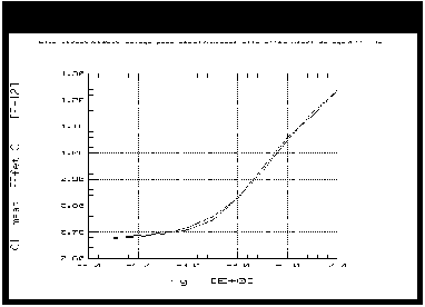
|
- Generally you will not need to change any of the optimization limits for these gate charge parameters. However, the limits are very important to the correct functionality of the optimizer.
Extracting Gm and Gds with ac_gm_gds
This is an initial extraction for Gm and Gds. These parameter values will be refined in a later procedure.
| 1 |
Locate the values for EEFET3.gmmaxac, gammaac, kappaac, peffac, and vtoac in the Parameters table. |
| 2 |
Select the setup ac_gm_gds, and Display Plots. |
| 3 |
From Extract/Optimize folder, select Init_dispersion and Execute. |
| 4 |
Select opt_gm_fet3 or opt_gm_hemt1, and Execute. Observe the changes in the plots and the Parameters table values. You probably will not need to change the optimization limits. |
- There may be a slight tradeoff in match between Gm and Gds. When the Gds data is well-matched the Gm data may degrade. You may like to perform the optimization again to see if it improves the match of both Gm and Gds. Or you can repeat both the Init_dispersion transform and the opt_gm transform.
- Note that Gm AC is lower than Gm DC because of trapping effects: this is not accounted for in most industry standard models.
Extracting Output Charge Parameters
The extraction procedures in the following setups use the S-parameter data you measured in the second Meas_Spars procedure. It is essential you use that S-parameter data, and not jump directly to these extractions using the wrong set of S-parameter data.
These procedures start by extracting the C21 and C22 capacitances, and then fit Cdso and Tau to the extracted C21/C22 data using optimization. The final procedure extracts the dispersion parameters.
Extracting the Linear Equivalent Circuit
| 1 |
From the AC_all DUT, select the Meas_Spars setup and Display Plots. |
| 2 |
From the Extract/Optimize folder, select mdl and Execute. This computes and saves a set of linear equivalent circuit parameters based on the S-parameters measured with bias. You will see the traces change on the plots, though a large amount of data is displayed and it is difficult to distinguish the convergence of individual traces. |
Extracting Initial Capacitance with Cgd_vgs_vds
This procedure extracts an initial value for the gate-to-drain capacitance.
| 1 |
Locate the values for deltds, lambda, and c12sat in the Parameters table. |
| 2 |
Select the setup Cgd_vgs_vds. |
| 3 |
From the Plots folder, select the Cgd plot, and Display Plot. |
| 4 |
From the Extract/Optimize folder, select the transform opt_to_Cgd and Execute. Observe the changes in the plot and in the Parameters table values. |
- Generally you will not need to change any of the optimization limits for these charge parameters. However, the limits are very important to the correct functionality of the optimizer.
Extracting Final Capacitance with Qg_vds_vgs
This procedures extracts final values for the capacitance parameters.
| 1 |
Locate the values for EEFET3.c11o and c11th in the Parameters table. |
| 2 |
Select the setup Qg_vds_vgs. |
| 3 |
From the Plots folder, select the C11 plot, and Display Plot. |
| 4 |
From the Extract/Optimize folder, select the transform opt_C11_Cgd and Execute. You will see the traces converge on the plot, and the parameter values may change in the table. You probably will not need to change any of the optimization limits. The following figure illustrates a typical C11 plot. |
Figure 149 Example C11 Device Input Capacitance Plot
|
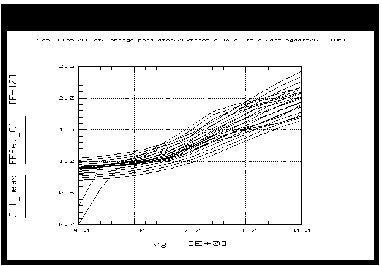
|
- The C11 plot shows how the input capacitance values trend upward vs. Vgs from threshold, spreading as they go toward the upper limits.
| 5 |
Note the values for EEFET3.c12sat and cgdsat in the Parameters table. |
Extracting Tau and Ri with Tau_Ri
The extractions for Tau and Ri are grouped together, even though they are independent, because both parameters are dependent on good extraction of the extrinsic and package parasitics. Tau is the time constant delay of S21. It is hard to separate from the transcapacitance Cds, the output capacitance with a change in input voltage.
| 1 |
Locate the values for EEFET3.tau and cdso in the Parameters table. |
| 2 |
Select the setup Tau_Ri_Cds. |
| 3 |
From the Plots folder, select the Tau and Cds plots, and Display Plot. |
| 4 |
From the Extract/Optimize folder, select the opt_Tau transform and Execute. This optimizes both Tau and Cds. Observe the data change on the trace, and possible parameter value changes for EEFET.tau and cdso. The following figure illustrates an example of plotted Tau data. The spread in data is caused by capacitance effects. |
Figure 150 Example Tau Plot
|
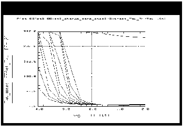
|
- If the Tau extraction yields a parameter value of zero or less, the problem may be in the earlier parasitic extractions. If the parasitic extractions look good and the Tau extraction looks bad, set a value for Tau manually. A good nominal value is 5.0 picoseconds for a 0.5 um GaAs FET, scaled approximately linearly with gate length for other FETs.
| 5 |
Close the Tau and Cds plots. Display the Ri plot. |
| 6 |
Locate the value for EEFET3.ris in the Parameters table. |
| 7 |
Select the opt_ri transform and Execute. Observe the data change on the trace, and a possible parameter value change for EEFET3.ris. The following figure illustrates example Ri data. |
Figure 151 Example Ri Plot
|
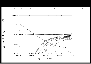
|
- If the Ri extraction yields a value of zero or less, it indicates that the contact resistance Rg was extracted too high. If this is the case, you may wish to re-iterate the rg_rd extraction for more accurate results. Ri is typically a value of only a few ohms, which may erroneously be attributed to Rg. The effect may be unimportant if the total of the gate resistances is good. If the fit of total gate resistance to S11 is sufficiently good the iteration of the rg_rd contact resistance extraction is not necessary.
- You can also reset the value of EEFET3.rg in the Parameters table a little lower, forcing the remaining resistance to be attributed to Ri. If you do this, or if you re-iterate the rg_rd contact resistance extraction, you must perform the mdl transform in the second Meas_Spars setup again before performing the opt_ri transform in this setup. Then check the Parameters table values for Ri again.
Extracting Dispersion Parameters
Both Gm and Gds change in GaAs devices due to traps and other effects. This procedure adjusts the dispersion parameters that model this behavior. The setup used in this extraction is tied to the S-parameter measurement and linear equivalent model extracted in the second Meas_Spars setup. The mdl transform in that setup must be active (that is, no other S-parameters must be measured and no other mdl transform must be run since the one in the second Meas_Spars setup).
| 1 |
If the mdl transform in the second Meas_Spars setup has not been run, open that setup and Execute the transform. |
| 2 |
Scroll the Parameters table to show some of the following parameters: EEFET3.gmmaxac, gammaac, kappaac, peffac, vdeltac, gdbm, kdb, and vdsm. You will not be able to display them all at the same time. |
| 3 |
Select the setup ac_gm_gds. |
| 4 |
From the Plots folder, select Gm plot, and Display Plot. |
| 5 |
From the Extract/Optimize folder, select the transform opt_gm_fet3 or opt_gm_hemt1, and Execute. Observe the traces converge on the plot, and the parameter values change in the table. The following figure illustrates example Gm data. Some dynamic thermal effects may be observed. |
Figure 152 Example Gm Plot in the ac_gm_gds Setup
|
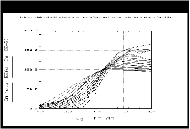
|
- You can use the X-low/X-high function if you want to optimize over only a portion of the trace.
| 6 |
Scroll the Parameters table to show more of the relevant parameters. |
| 8 |
Select the opt_gds transform, and Execute. Observe the traces converge on the plot, and the parameter values change in the table. The following figure illustrates example Gds data. |
Figure 153 Example Gds Plot in the ac_gm_gds Setup
|
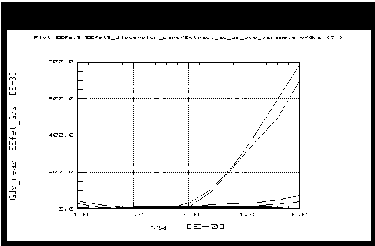
|
- In some cases there may be a tradeoff between a good data fit at threshold and in the active region of operation.
Verifying the Model Against the Measured Data
This procedure uses the File_Validate setup to verify that modeled S-parameter data is comparable to measured data. An S-parameter measurement is performed at one bias value—the specific bias of expected device operation. This allows a single bias condition to be isolated for comparison purposes, which cannot be done with the multiple-bias conditions of earlier S-parameter measurements.
Defining the Instrument States
To define the DC Source/Monitor instrument state, follow these instructions:
Use the same DC source/monitor and network analyzer settings as you did for the Meas_Spars and other S-parameter measurements. Then return to this chapter and continue.
The Input Variables
| 1 |
From the Utilities DUT, select the File_Validate setup and observe the inputs. The following figure illustrates the inputs used in this measurement. |
Figure 154 Inputs for Verification Data
|
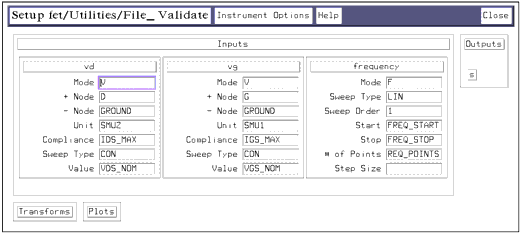
|
| |
• |
The frequency inputs are set the same as for the other S-parameter measurements. |
| |
• |
The gate voltage is set for a CONstant value of VGS_NOM, the value of Vgs that gives an Ids value representative of actual device operation. |
| |
• |
The drain voltage is set for a CONstant value equal to the intended Vds of device operation. |
Measuring and Plotting
| 1 |
With the File_Validate setup selected, select Display Plots, then click Measure. |
| 2 |
From the Extract/Optimize folder, select mdl and Execute. This embeds the extrinsic elements and makes the model parameters comparable with the measured results. |
| 3 |
Observe the measured and modeled S-parameter data on the plots. The plot below illustrates typically well-converged data. |
Figure 155 Measured and Modeled S11 and S22 Data
|
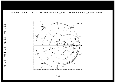
|
Storing the Model
This procedure stores the model in IC-CAP, including all the device-specific measured and simulated data. Once you have developed the device model, it can be used as a component in the Agilent RF and Microwave Design System (MDS). You can use it for circuit simulation, inserting it into circuits under design to emulate the characteristics of your device.
If you will be modeling large numbers of devices, it is worthwhile to organize your directory structure according to device type, geometry, and batch or wafer.
| 1 |
Decide where in your directory structure you intend to store this model file. |
| 2 |
From the IC-CAP/Main window select Model, then select File > Save As from the pulldown menu. A dialog box is displayed. |
| 3 |
Select a new filename that associates this model with the device, for example eefet6_9jun95.mdl. Type the full directory pathname and the filename into the dialog box. |
| 4 |
Select OK or press Return to store the data and close the dialog box. |
Saving the Parameters for Series IV Compatibility
A transform in the File_Validate setup lets you save the model parameters in a format that can be used by the Series IV Design System.
| 1 |
From the DUT/Setup panel select the File_Validate setup. |
| 2 |
From the Extract/Optimize folder, select the transform SaveFile, and Execute. |
| 3 |
Type a filename for the parameters and click OK. The parameters will be saved in a Series IV-compatible format. The format is MDIF (measurement data interchange format). When the transform is run, a copy of the MDIF file is written to the UNIX standard out window. |
Saving the Parameters in SPICE Format
You can also save the list of individual model parameters in SPICE format for later access. These parameters can be read directly into MDS.
| 1 |
From the Model window choose File > Export Data > Extracted Deck. Select a new filename, for example fet6pars.mdl. Type the full pathname and your filename into the dialog box. |
| 2 |
Click OK or press Enter to store the parameters in SPICE format. |
This completes the example high-frequency EEfet3 measurement and parameter extraction procedure. For an explanation of how to use IC-CAP model data in MDS, refer to Appendix D, "Using IC-CAP Data with MDS."
|