Using the Agilent Root Diode Model
This chapter provides an example procedure that takes you step-by-step through a measurement and model generation. Much of the data used in this procedure is taken from a diode in a two-port configuration, with some reference to a one-port configuration also. Values you use in generating your own device model will depend on the configuration and the particular characteristics and compliance values for your device: use its data sheet (if available) as a reference.
This example is provided as a starting point. It is a straightforward procedure that uses only a subset of IC-CAP's total capabilities. The complete procedure documented gives all the steps necessary to configure IC-CAP with the parameters for preverification measurements, ideality and parasitic extractions, and the main data acquisition and model generation.
|
Note
|
|
|
|
|
Although you will modify the variable values in factory default files during this procedure, do not under any circumstances change the names of any variables or setups. These names are used by the software in the data acquisition and model generation process.
|
|
The example procedure gives detailed instructions on how to:
| • |
Initialize device parameters. |
| • |
Measure and extract the system measurement port series resistances. |
| • |
Make a DC measurement to preverify device DC performance. |
| • |
Calibrate the network analyzer. |
| • |
Make an S-parameter measurement to preverify device performance at high frequencies. |
| • |
Measure and extract the ideality factor. |
| • |
Measure and extract the device parasitic resistances and inductances. |
| • |
Set up the parameters for the main data acquisition and model generation |
| • |
Initiate the main data acquisition. Plot the measured data. |
| • |
Initiate the model generation. Plot the calculated state functions. |
| • |
Verify the model against measured data. |
| • |
Store the data and model files for circuit simulation in Agilent MDS. |
Where necessary, other chapters are cross-referenced at appropriate points in the procedure, so that you will have the information you need for system hardware setup and calibration at the proper times.
|
Note
|
|
|
|
|
Measurement parameters and measured data are specific to individual devices. Information and data are provided here as examples and guidelines, and are not intended to represent the only correct results.
|
|
The procedure provides guidelines on setting values to measure your device. However, the values you use will be based on your knowledge of your device and on information in its data sheet (if available), as well as on the guidelines presented here: they may or may not correspond with the example values.
The illustrations of plotted data are provided as visual examples of possible results. They are not intended to represent a single device, nor do they necessarily correspond with the values given in the procedure. The plots can be used to check the reasonableness of your own data, which should appear similar in shape but not necessarily coincident in values.
The DUT and Setups
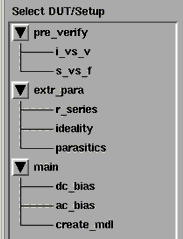
The Model window is the central access point for the measurement and model generation procedures. The Model window includes the DUT/Setup panel and the file tabs to access the Model Parameters table, the model variable table, and other IC-CAP features.
The illustration shows the DUT/Setup panel for this model. The DUTs (for example pre_verify), indicated by the inverted triangles, are groupings of similar measurement setups used for related measurements, or to extract related model parameters. The setups (for example i_vs_v) contain the information used to define the inputs and outputs for each measurement, as well as their measurement hardware configurations and their associated transforms and plots.
Figure 92 Agilent Root Diode DUT/Setup Panel
|
|
The list of macros available from the Macros tab provides access to functions that combine certain groups of IC-CAP operations into single operations.
Initializing Device Parameters
You begin the procedure by giving the device an identifier, and entering the configuration (number of ports, two-port or one-port) and device current limits. For this you use the init_val macro and the model variable table. The model uses the current limits to set a safe operating range for the measurements, and measures only within that range. When the init_val macro is executed, it also initializes internal program functions that are essential in the model generation process, and it provides annotations for the data plots.
| 1 |
Click the Macros tab to display the names of the macros. |
| 2 |
In the Select Macro list, select init_val, then Execute. A dialog box is displayed, asking you to enter a device identifier. |
| 3 |
Enter a name to identify the device under test, then select OK or press Return. |
| 4 |
The next dialog box asks you to input the device area (that is, the cross-section of the diode) in square meters. The device area obviously will be a very tiny value, perhaps in the region of 200 um*50 um = 1e-8. This area value is required for interface of the finished model with MDS. |
| 5 |
Another dialog box asks you to enter a directory name. Either select OK if you wish to store the model files in the directory shown, or backspace over the directory name and type in the name of another existing directory. |
| 6 |
The next dialog box asks you to specify the number of device ports. |
| |
• |
If the device is in a two-port configuration, type 2. |
| |
• |
If it is one-port, type 1. |
- If you try to enter a number other than 2 or 1, a message in the IC-CAP/Status window will tell you the number of ports must be 1 or 2.
| 7 |
The macro is executed, and values you selected are entered in the model variable table. Open the model variable table by clicking the Model Variables tab. |
|
Note
|
|
|
|
|
Do not edit the init_val macro. It contains executable code.
|
|
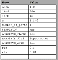
Setting the Current Limits
You use the model variable table to set the forward and reverse current limits to be used in measuring your device. To edit the variable table, move the mouse pointer to the appropriate variable value, click left, and move the pointer over the old information to highlight it. Then type in the new value over the old.
| 8 |
For the value of IFwd, enter the maximum forward conducting current for your device. Use the device data sheet, if available, to look up the value. |
| 9 |
For the value of IBrk, enter the maximum diode breakdown current value (usually less than 1/10 IFwd). |
| 10 |
Do not change the other values in the table at this time. |
Figure 93 Model Variable Table
|
|
| 11 |
You can display the variable table in a separate window by selecting Detach. Resize the window and move it to a convenient place away from the central work area. |
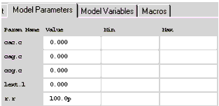
Values in the Parameters Table
The figure below illustrates the Model Parameters table, with the initial values for the extrinsic parasitic capacitances, inductance, and resistance. The table is presented so that you can enter values for these extrinsic parasitics based on your knowledge of the device, or on estimates, or on measurements of the open fixture. In addition, you can set limits by entering minimum and maximum values for each parameter. Parameter values that are outside their limits are clamped to their minimum or maximum values.
Figure 94 Model Parameters Table
|
|
| 1 |
To access the Parameters table, click the Model Parameters tab. |
| 2 |
To change a value in the Parameters table, move the mouse pointer over the current entry and click left to highlight it, then type in a new value. |
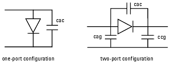
| 3 |
The default for all the c values is 0.000, for both a one-port and a two-port configuration. You can change the value of cac.c for either a one-port or two-port configuration. For a two-port configuration you can also change the values of cag.c and ccg.c. However, the program always uses zero values for cag and ccg in a one-port configuration, even if you manually change the values in the table, since there is no parasitic capacitance from anode to ground or from cathode to ground. |
- A reasonable capacitance value to enter for a pad on a wafer is 50 fF.
- The figure below is a schematic representation of the extrinsic capacitances. Note that the cathode must be grounded in the one-port configuration.
Figure 95 Schematic Diagram of Extrinsic Capacitances
|
|
| 4 |
lext.l is the bond inductance. The default value is 0.000. If you know or can estimate the bond inductance for your device based on wire length or grid size, enter an appropriate value. |
| 5 |
r.r is not a real resistance, and is not associated with the measurement system or the diode. It is an artifact used by IC-CAP for verification in a one-port configuration because IC-CAP by default recognizes a two-port configuration. It is set to an initial default value of 10.00 G for a two-port diode configuration. For a one-port configuration, it is set to a very small value such as 100.0 p. for a two-port diode configuration. For a one-port configuration, it is set to a very small value such as 100.0 p. |
Extracting the Measurement Port Series Resistances
This procedure need be performed only following initial installation of the system or if changes are made in the system hardware.
The procedure measures a short circuit at the normal device measurement interface plane. IC-CAP controls the DC source/monitor to force a current and monitor the voltage. The primary measurement is at port 1, and the port 2 measurement is synchronized to the port 1 measurement. You set the measurement parameters by defining the instrument state and the DC input values, as explained in the next pages.
The software calculates the series resistances from the outputs of the bias networks to the inputs of the device under test. The resistance values are then incorporated into the model file, and their effects are removed from the device response during the modeling process. (The default port resistance for both port 1 and port 2 is 0.) If the diode under test is in a two-port configuration, the series resistance is calculated for both measurement ports; for a one-port configuration, only the port 1 resistance is calculated, and the port 2 resistance is set to 0. (The anode must be connected to port 1.)
Note that the first part of the procedure differs for probe station and in-fixture measurements.
Setting Up for the Measurement
| 1 |
If you are using a probe station, position an impedance standard substrate (ISS) on the chuck. For a two-port configuration, place both the port 1 and port 2 probes on a short circuit standard. For a one-port configuration, the placement of the port 2 probe is irrelevant--it need not be lowered. |
| 2 |
If you are using a fixture, insert the short from the in-fixture calibration kit. |
| 3 |
From the DUT/Setup panel select the r_series setup. |
Defining the DC Source/Monitor Instrument State
Follow the steps described in the appropriate chapter shown next:
Set Integ Time to M (medium). Then return to this chapter and continue.
Setting the r_series Input Values
Use the following guidelines to set the inputs (most will not need to be changed from the factory settings):
Table 30 For the ia input
|
|
Mode
|
I
|
To Node
|
A (anode)
|
From Node
|
GROUND
|
Compliance
|
as 5 to 10V, because the device is not yet connected
|
Start, Stop
|
current values that define a current range within the limits of the bias network
|
# of Points
|
a value sufficient to make several measurements across the current range
|
The Step Size will be set automatically
|
| • |
The Unit name must match the name of the SMU connected to the device anode (probably VA). This is also the SMU unit name you set in the hardware window. Refer to the appropriate chapter as follows: |
| • |
With a current input, compliance refers to voltage. |
|
Caution
|
|
|
|
|
The bias networks can be destroyed if IC-CAP measurement current values are set too high. Be sure you know the maximum current ratings of your bias networks, and do not set current values beyond these limits. (The standard bias networks for the Agilent 85122A and 85123A parameter extraction test systems are rated at 0.5 amp.)
|
|
Table 31 For the ic input
|
|
Mode
|
I
|
To Node
|
C
|
From Node
|
GROUND
|
Unit
|
VC
|
Compliance
|
the same as for ia
|
Sweep Type
|
SYNC
|
Ratio
|
Number_of_ports-1, so that for a two-port configuration the ratio is 1 and a synchronized ic sweep is measured. For a one-port configuration the ratio is 0, therefore no ic sweep occurs and the port 2 series resistance retains the default value of 0
|
Offset
|
0.0
|
Master Sweep
|
ia, so that the ic sweep is synchronized to the ia sweep
|
| • |
The Outputs are factory set, and should not be changed. |
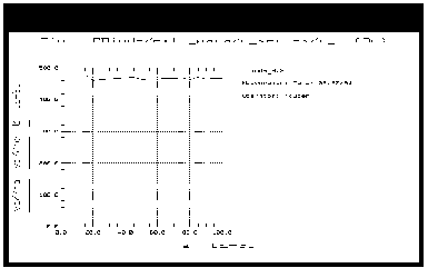
Measuring and Extracting
| 1 |
Under Measure/Simulate select Measure. |
| 2 |
When the measurement is complete, the Measuring light on the DC source/monitor goes out and the IC-CAP wristwatch icon disappears. |
| 3 |
Select the Extract/Optimize tab. |
| 4 |
Select compute_rseries > Execute. The transform calculates the port series resistances from the measured data and enters the values into the model variable table as r1s and r2s. |
| 5 |
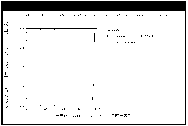
To view a plot of the data, select Plots > r_i > Display Plot. The figure illustrates the voltage/current data for a one-port diode configuration. The va/ia (port 1) data is plotted across the measured bias range. The vc/ic (port 2) data has a zero value across the range for a one-port device. |
Figure 96 Example r_i Data for a One-Port Configuration
|
|
Installing the Device
|
Caution
|
|
|
|
|
Ground yourself with an antistatic wrist strap to reduce the chance of electrostatic discharge. (Note that the Agilent 85122 or 85123 system work surface is coated with antistatic material and is connected to chassis ground, therefore a static mat is not required.)
|
|
Install the diode carefully on the probe chuck or in the fixture. To install the diode in a two-port configuration, connect the anode to port 1 and the cathode to port 2. To install the diode in a one-port configuration, connect the anode to port 1 and the cathode to ground. A configuration with the anode grounded is NOT supported. Be sure to handle the device as little as possible, to avoid damaging it. Once the device is in place, avoid bumping the test station.
|
Caution
|
|
|
|
|
Remove any high-intensity light sources such as microscope light before taking a measurement. One simple method of blocking light is to place an opaque box on the fixture directly above the device.
|
|
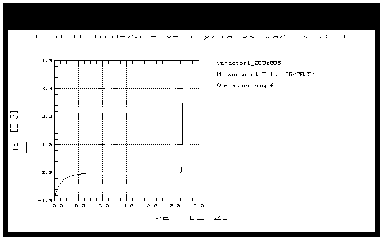
Preverifying the Device DC Data
This procedure uses the i_vs_v setup to measure the current values with respect to voltage. It is an opportunity to take a first look at the device performance and explore its characteristics. The procedure starts with conservative values, and iteratively expands the voltage range until it sweeps from breakdown to the voltage where forward conducting current is maximum. This also lets you select the most appropriate measurement range for the main data acquisition and other measurements.
This is a quick way to verify that the device DC characteristics are good, before starting a complete data acquisition and modeling procedure. The data from this measurement can also be used for later comparison with data predicted by the generated model. It is not necessary to do the preverification measurement every time you perform a model generation, especially if you are using a data sheet.
Defining the DC Source/Monitor Instrument State
Follow the same process you used in the r_series measurement. Use the same settings.
Setting the i_vs_v Input Values
This procedure defines the input signals to be applied to the device under test for the DC preverification measurement.
The actual settings you use will be dependent on your device and on the range of measurements you wish to take.
- If you are measuring a series of devices of the same type and have already set the input values, go directly to Measuring and Plotting. Otherwise, select the i_vs_v setup and use the following settings as guidelines:
Table 32 For the va input
|
|
Mode
|
V (voltage)
|
To Node
|
A (anode)
|
From Node
|
GROUND
|
Compliance
|
See note below.
|
Sweep Type
|
LIN to provide a linear voltage sweep from start to stop voltage values
|
Start, Stop
|
In setting the range, unless you know the operating voltage range of the device, it is best to begin with conservative values to let you observe the device response. Begin by setting a Start value of 0.0 or a slightly negative value. Similarly, begin with a conservative Stop value. If you do know the operating range of the device, you may want to use less conservative values.
|
# of Points
|
A value sufficient to clearly display the measurement results.
|
The Step Size is calculated automatically in software from the start/stop values and number of points.
|
Table 33 For the vc input
|
|
Mode
|
V (voltage)
|
To Node
|
C
|
From Node
|
GROUND
|
Unit
|
VC
|
Compliance
|
See note below.
|
Sweep Type
|
CONstant
|
Value
|
0 to ground the cathode
|
| • |
The Unit names must conform to the names you set in the hardware window when you configured IC-CAP to recognize the system hardware (probably VA and VC). They must also correspond with the actual SMU connections from the Agilent 4142. |
| • |
You provide Compliance values to limit SMU output voltage or current and thus prevent damage to the device under test, as well as to the SMUs, bias networks, and probes, if used. With a voltage input, compliance refers to current: in general, you can set both the va and vc Compliance to IFwd, the forward conducting current value you set in the model variable table. |
- However, in setting compliance values, consider this issue: compliances are physically different in the forward and reverse bias ranges. It is important to make sure the compliance is not set too large for breakdown. Although you set only one compliance value for a setup, you are actually sweeping over two ranges, the negative range and the positive range. Two alternatives are possible to overcome this issue: either you can run two setups, one for the forward measurement using IFwd as the compliance value, and one for the reverse measurement using IBrk as the compliance value. Or you can run a single setup, making the va Start value so slightly negative at the first iteration that it will not allow the device to reach breakdown.
| • |
The Outputs are factory set, and should not be changed. |
Measuring and Plotting
This procedure triggers the device measurement, controlling the DC source/monitor to supply the signals you defined in the instrument options window and the inputs, and monitors the results.
|
Note
|
|
|
|
|
Be sure to keep a UNIX window open so that you will see any compliance error that may be reported by the DC source/monitor. If so, you may need to reduce the value of IFwd you set in the model variable table.
|
|
|
Note
|
|
|
|
|
Before making the DC measurement, manually put the network analyzer in hold sweep mode by pressing STIMULUS > MENU > MORE > HOLD on an Agilent 8510, or MENU > TRIGGER MENU > HOLD on an Agilent 8753.
|
|
| 1 |
Select Plots > i_v > Display Plot. |
| 2 |
Select Measure/Simulate > Measure. When the measurement is complete, the Measuring light on the DC source/monitor goes out, the IC-CAP wristwatch icon disappears, and the measured data is displayed in the plot window. |
Figure 97 Example DC Measurement of Current vs Voltage
|
|
| 3 |
Check the plot. The objective of this measurement is to show the device response from breakdown to maximum forward conducting current, as in the illustration. If your plot shows only a partial device response you will need to change the inputs and repeat the measurement, as follows: |
| 4 |
Go back to the inputs. If necessary, change va Start to a lower value to measure more of the device breakdown characteristics; or change Stop to a higher value to measure the forward conducting current. Select Measure again. |
| 5 |
Iterate as necessary until you have measured a complete device response. |
| 6 |
If the measured data looks wrong for your device, check the probe contacts, the bias connections, and the measuring instruments. Make sure the device is oriented properly, with the right ports connected to the right terminals (anode to port 1, cathode to port 2 for a two-port device; anode to port 1, cathode to ground for a one-port device). If none of these resolves the problem, the device may be defective. |
| 7 |
To save the measured data select File > Save As and a filename with the suffix .set (for example dc_test.set). Then select OK. |
Calibrating the Network Analyzer
It is important to calibrate the network analyzer before you perform any S-parameter measurements. Good calibration of the network analyzer is critical to a good measurement and extraction. This procedure uses a frequency list calibration.
Frequency List Mode
Frequency list lets you define an arbitrary list of frequencies in one or more segments. During the measurement sweep the synthesizer is phase-locked at each frequency point, as in the stepped-sweep mode. For the purposes of this model, you will define one frequency segment in the list with a frequency range at least as wide as the operating range of the device. This calibrated swept frequency range will be used for all the S-parameter measurements: the AC preverification, parasitics, and main data acquisition measurements. The model will be generated at one of the calibrated frequencies in the list.
The advantage of frequency list mode for use in a table-based model such as this is that it lets you define a smaller number of measurement points than for a step or ramp frequency cal. This reduces the total measurement time, particularly in the main data acquisition where measurements are taken at all the bias points at each frequency in the list. A # of Points of 5 to 13 provides adequate measurement resolution as well as a quite fast total measurement time for the main data acquisition.
Frequency list calibration procedures for an Agilent 8510-based system and an Agilent 8753-based system are given in the next few pages.
Connecting the Network Analyzer
If you have not already done so, connect the RF cables from the network analyzer test ports to the RF inputs of the bias networks. When it is time to measure the calibration standard devices, connect them to the DC/RF ports of the bias networks.
Frequency List Calibration for an Agilent 8510-Based System
If you are using an Agilent 8510-based system, follow the steps below.
| 1 |
On the network analyzer, press LOCAL to gain front panel control. Press PRESET to return to a known standard state. |
| 2 |
To define a linear frequency list, on the network analyzer in the STIMULUS area press MENU > MORE > EDIT LIST > CLEAR LIST > YES > ADD. A default frequency list segment is presented. |
| 3 |
To change the segment to your chosen frequency range press SEGMENT: START, and use the numerical keypad to set the start frequency, ending with one of the terminator keys (such as M/ ) at the right of the keypad. Similarly, press STOP and set the stop frequency. ) at the right of the keypad. Similarly, press STOP and set the stop frequency. |
|
Note
|
|
|
|
|
Use the SEGMENT: START and STOP softkeys, not the START and STOP hardkeys in the STIMULUS area of the front panel.
|
|
| 4 |
Press SEGMENT: NUMBER of POINTS, and enter the number of frequency points to be measured across the range, then press the x1 terminator key. Keep in mind that the fewer the number of points, the less time the measurements take. |
| 5 |
Press DONE to return to the frequency list menu. The segment you just defined is listed on the screen. |
| 6 |
Press DONE to return to the main stimulus menu. Press FREQUENCY LIST > SINGLE SEGMENT to activate the frequency list mode and set the analyzer to sweep the segment you defined. |
| 7 |
Press MENU > MORE > CONTINUAL to set a continual stimulus sweep. |
| 8 |
Press MENU > POWER MENU and set the desired power level, then press the x1 terminator key. In setting the source power and attenuation, take care that the power level will not be excessive at the device input. Also consider the gain of the device, and set a power level that will not saturate the input port samplers of the analyzer. If the power level at the sampler goes above -8 dBm, an IF OVERLOAD error message is displayed and you will need to reduce the source output power. The default network analyzer power level is 0 dBm. |
| 9 |
For a device with power drop-off at higher frequencies, you may wish to set a power slope using the stimulus menus. An appropriate power slope would be in the region of 2-3 dB/GHz. |
| 10 |
In the RESPONSE area, press MENU > AVERAGING ON/restart, and enter an averaging factor high enough to reduce trace noise and increase dynamic range as appropriate for your device measurements. Although the default is 256, you may wish to use an averaging factor as low as 16 to reduce overall measurement time. |
| 11 |
If the cal kit constants for your calibration kit are not loaded into the network analyzer, load them from disc now by pressing DISC > LOAD and specifying the data type and file name. |
| 13 |
Press CAL > CAL1 or CAL2 (depending on your cal kit), and perform a two-port calibration, measuring each of the standard devices in turn and pressing the softkeys as each measurement is complete. |
|
Note
|
|
|
|
|
IC-CAP does not support a one-port cal: therefore you must perform a two-port cal for either a two-port or a one-port device. If you try to do a one-port cal, IC-CAP will display anomalies and error messages.
|
|
| 14 |
At the end of the calibration sequence, the cal set numbers are listed in the softkey menu. Press CAL SET 1 to store the calibration in cal set #1. (Or use another available cal set.) |
CW Calibration Subset for an Agilent 8510-Based System
| 1 |
To create a CW frequency subset of the broadband frequency list calibration, press CAL > CORRECTION ON > CAL SET 1 (this turns on the broadband cal you just completed), then MORE > MODIFY CAL SET > FREQUENCY SUBSET. Use the SUBSET: START and SUBSET: STOP softkeys in the SUBSET menu (NOT the front panel keys) to set both start and stop to the same frequency. |
| 2 |
Press CREATE & SAVE, and store this calibration in cal set #2 or another available cal set. |
| 3 |
Note the numbers of the cal sets where you save the calibrations: you will need to list one of these numbers as part of the instrument state for each of the network analyzer measurements. |
|
Note
|
|
|
|
|
For more detailed information, refer to the Agilent 8510 Operating and Programming Manual.
|
|
Frequency List Calibration for an Agilent 8753-Based System
If you are using an Agilent 8753-based system, follow the steps below.
| 1 |
On the network analyzer, press LOCAL to gain front panel control. Press PRESET to return to a known standard state. |
| 2 |
If you are using a system with the 6 GHz receiver option and you wish to measure in the 3 GHz to 6 GHz range, press SYSTEM > FREQ RANGE 3GHz6GHz. |
| 3 |
To define a linear frequency list, on the network analyzer press MENU > SWEEP TYPE MENU > EDIT LIST > CLEAR LIST > YES > ADD. A default frequency list segment is presented. |
| 4 |
To change the segment to your chosen frequency range press SEGMENT: START, and use the numerical keypad to set the start frequency, ending with one of the terminator keys (such as M/) at the right side of the keypad. Similarly, press STOP and set the stop frequency. |
|
Note
|
|
|
|
|
Use the SEGMENT: START and STOP softkeys, not the START and STOP hardkeys on the front panel.
|
|
| 5 |
Press SEGMENT: NUMBER of POINTS, and enter the number of frequency points to be measured across the range, then press the x1 terminator key. Keep in mind that the fewer the number of points, the less time the measurements take. |
| 6 |
Press DONE to return to the edit list menu. The segment you just defined is listed on the screen. |
| 7 |
Press DONE to return to the sweep type menu. Press LIST FREQ > SINGLE SEG SWEEP to activate the frequency list mode and set the analyzer to sweep the segment you defined. |
| 8 |
Press RETURN > RETURN > TRIGGER MENU > CONTINUOUS to set a continuous stimulus sweep. |
| 9 |
Press MENU > POWER and set the desired power level, then press the x1 terminator key. In setting the source power and attenuation, take care that the power level will not be excessive at the device input. Also consider the gain of the device, and set a power level that will not saturate the input port samplers of the analyzer. If a receiver input is overloaded (>+14 dBm), the analyzer automatically reduces the output power of the source to -85 dBm and displays the error message OVERLOAD ON INPUT (R, A, B) POWER REDUCED. In addition, the annotation P appears in the left margin of the display to indicate that the power trip function has been activated. When this occurs, reset the power to a lower level, then toggle the SOURCE PWR on/off softkey to switch on the power again. appears in the left margin of the display to indicate that the power trip function has been activated. When this occurs, reset the power to a lower level, then toggle the SOURCE PWR on/off softkey to switch on the power again. |
| 10 |
Press AVG > AVERAGING FACTOR, and enter an averaging factor high enough to reduce trace noise and increase dynamic range as appropriate for your device measurements. A good default averaging factor is 256. To speed your measurements, you may find it convenient to set an averaging factor as low as 16. Press AVERAGING ON. |
| 11 |
You can further reduce the noise floor by reducing the receiver input bandwidth. Press IF BW in the average menu, and enter one of the following allowed values in Hz: 3000, 1000, 300, 100, 30, or 10. A tenfold reduction in IF bandwidth lowers the measurement noise floor by about 10 dB; however, the sweep time may be slower. For more information on averaging and the different trace noise reduction techniques, refer to the Agilent 8753 operating manual. |
| 12 |
Press CAL > CAL KIT, and select the appropriate default or user-defined cal kit for your calibration devices. |
| 14 |
Press CAL > CALIBRATE MENU, and perform a two-port calibration at the analyzer front panel, measuring each of the standard devices in turn and pressing the softkeys as each measurement is complete. A TRL* or LRM* cal is an appropriate alternative for in-fixture measurements (see Appendix C, "Using IC-CAP with an Agilent 85123A Device Modeling System"). Omit isolation cal. Press DONE, and save the cal in the register number specified in the instrument options table. |
| 15 |
Detailed procedures for measurements of calibration standards are provided in the Agilent 8753 operating manual. |
CW Calibration for an Agilent 8753-Based System
Refer to Appendix C, "Using IC-CAP with an Agilent 85123A Device Modeling System" for a CW calibration procedure that can be used for a system with an Agilent 8753 or 8720 network analyzer.
Preverifying the Device S-Parameter (AC) Data
This procedure uses the s_vs_f setup to measure the device S-parameters across a calibrated frequency range, at several bias points in the normal operating range of the device. It can use the measured DC preverification data for reference in choosing DC bias points of interest to you.
The procedure can be used as a quick check that the device performance is good at higher frequencies, before you do a complete data acquisition and model generation. It is not necessary to do the preverification every time you generate a model, especially if you are using data sheet values.
Defining the Instrument States
Select the Instrument Options tab and follow the steps described in the appropriate chapter shown next (with the exceptions noted below):
Because you used a frequency list cal rather than a swept frequency cal, note the following:
| • |
Be sure the instrument states you set for the network analyzer correspond to the values you set in your calibration. |
| • |
Be sure to set the averaging factor the same as in your calibration. |
| • |
Set Cal Type [SHN] to H for hardware. |
| • |
Set Cal Set No to the cal set or register where you stored your calibration. |
| • |
Set Use Linear List to Yes. |
Then return to this chapter and continue.
Setting the s_vs_f Input Values
This procedure defines the input signals from both the DC source/monitor and the network analyzer for this measurement.
| 1 |
Select the s_vs_f setup. |
| 2 |
Set the vc inputs the same as for the i_vs_v setup. |
| 3 |
In the va inputs set Sweep Type to LIST, and Sweep Order to 2. |
| 4 |
In list sweep mode, IC-CAP lets you specify up to 15 bias voltage values for the measurement. Using your measured DC preverification data as a reference, choose values of interest to you. For example, you might want to view the device response at bias points close to breakdown or in the forward conducting region. |
- Be conservative in setting the va Values. Note that the values must be monotonic (set in increasing order, not mixed at random).
| 5 |
The number of Values must equal the number of values you enter into the list. (This does not include any 0.000 values at the end of the list.) |
| 6 |
Set the freq Mode to F, Sweep Type to LIN, and Sweep Order to 1. |
|
Note
|
|
|
|
|
If you set a MHz value, write MEG in full. IC-CAP is not case-sensitive, and assumes that m or M corresponds to milli. If an error message is displayed during the measurement that indicates a network analyzer frequency value is too low, you may have entered M only.
|
|
| 7 |
Set the freq Start and Stop values to correspond with the frequency range of your calibration. |
| 8 |
Set the # of Points to correspond with the calibration. The step size is set automatically. |
Measuring and Plotting
|
Note
|
|
|
|
|
Before performing the S-parameter measurements, manually take the network analyzer out of hold sweep mode. Press LOCAL. Then in the STIMULUS area press MENU > MORE > CONTINUAL on an Agilent 8510; or press MENU > TRIGGER MENU > CONTINUOUS on an Agilent 8753, to initiate continuous sweep.
|
|
| 1 |
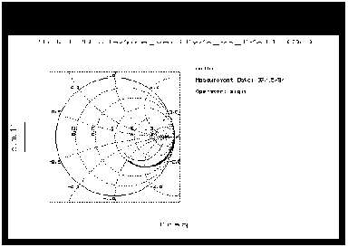
From the Plots tab, select sp > Display Plot. |
| 2 |
Select Measure/Simulate > Measure. |
| 3 |
Check the plot. The S-parameter data displayed should be typical for your device. The illustration shows example measured S11 data. If your device is in a two-port configuration, S22 will also be plotted. |
| 4 |
If the results are unexpected, recheck the values you set in the inputs and instrument options. In particular, be sure the instrument states and input stimulus signals match the values set in the network analyzer calibration. |
Figure 98 Example Measured S11 Data
|
|
| 5 |
If you change the inputs or instrument states, repeat the measurement. If the data still looks abnormal, the device may be defective and may need to be replaced with an acceptable one. |
| 6 |
To save the measured data, select File > Save As, type in an appropriate filename (for example spar_test), and select OK. |
If you are satisfied with the measured data for your device, continue with the procedures. Be sure the limits of the measurement domain are adequate: the domain should extend beyond the normal operating range of the device to show the limits of device behavior. If not, you may wish to redefine the voltage range you set in i_vs_v and s_vs_f, using values that are less conservative.
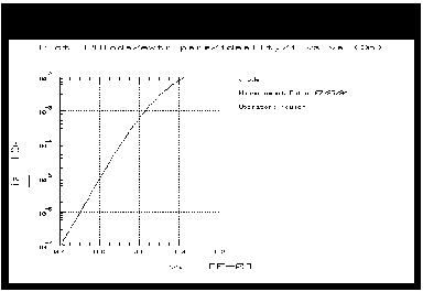
Measuring and Extracting the Ideality Factor
Ideality is the coefficient that multiplies Vthermal in the ideal diode equation. The diode resistance is approximated by the equation:
-

where n is the ideality factor, Vth is Vthermal (0.025V at room temperature), and I is the current.
In this setup, the diode is strongly forward biased. The current is swept from a very small positive current value up to maximum, to exercise the diode junction to include the region of its exponential behavior.
Defining the DC Source/Monitor Instrument State
Follow the same process you used in the r_series and i_vs_v measurements. Use the same settings.
Setting the ideality Input Values
Most of the input values for this measurement are factory preset and should not be changed. The current values are based on values you set in the model variable table at the beginning of the procedure. The other inputs are necessary to set up the required device measurement configuration. Select the ideality setup and use the following settings as guidelines.
Table 34 For the ia input:
|
|
Compliance
|
around the same value as the va Stop value used in the i_vs_v DC preverification or a little higher
|
Sweep Type
|
LOG scale to allow measurement of the inherently exponential distribution of points
|
Start and Stop
|
The purpose of the Start and Stop settings for ia is to force current from  0 amps to maximum. Stop is set to IFwd, which is the maximum forward conducting current value you set in the model variable table. Start is set equal to IFwd divided by some large number between 1000 and 10000. 0 amps to maximum. Stop is set to IFwd, which is the maximum forward conducting current value you set in the model variable table. Start is set equal to IFwd divided by some large number between 1000 and 10000.
|
Dec or Oct
|
Refers to a decade or octave log scale for plotted data. The correct setting for this measurement is D for decade.
|
| • |
When the ia Sweep Type is set to LOG, the input table automatically includes the fields Dec or Oct and Total Pts in place of Step Size. |
| • |
The number of points can be entered as either a # of Points per decade (as in this example) or a Total Pts across the sweep. |
Table 35 For the vc input
|
|
Compliance
|
See the note below.
|
Sweep Type
|
CONstant
|
Value
|
0.000, to ground the cathode
|
| • |
The vc Compliance value of 1.1*IFwd limits the current to a value 10% above IFwd to prevent damage to the device. |
| • |
The Outputs are factory set, and should not be changed. |
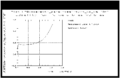
Measuring, Extracting, and Interpreting the Results
This procedure makes the measurement and computes the ideality factor from the results. The procedure explains how to check the measured data and computed ideality, and override the computed value if appropriate.
| 1 |
From the Plots tab. Select the N_vs_va plot, and Display Plot. |
Figure 99 Example Plot of Ideality vs Voltage
|
|
| 2 |
Select the Extract/Optimize tab. Select N > Execute. The transform calculates the ideality factor from the measured data and enters the value into the model variables table. |
| 3 |
To display the table, select the Model Variables tab. |
| 4 |
You can copy the model variables table in a separate window by selecting Detach. Resize the window and move it to a convenient place away from the central work area. |
| 5 |
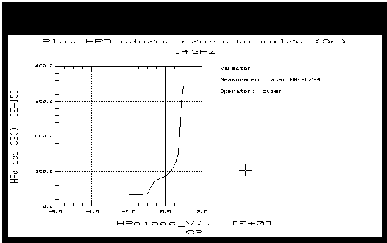
You can set the program to recompute the ideality factor from only the relatively linear portion of the measured data. Note that the linear region of the measurement is the region where the Rdiode equation given under Measuring and Extracting the Ideality Factor applies. The next steps use the X-low/X-high function to select a linear portion of the trace. |
| |
• |
Select Setup Variables. A variable table appears that lists X_LOW and X_HIGH with their default value of 0 or current values. |
| |
• |
Choose a relatively linear portion of the plotted trace. Click the mouse pointer at the lower and upper boundary points of the linear portion, to make a box on the trace as illustrated below. |
Figure 100 Choosing a Linear Portion of the Plotted Trace
|
|
| |
• |
From the plot menu select Options > Copy to Variables. This changes the X_LOW and X_HIGH values in the table to the boundary points you selected. |
| 6 |
Select Extract/Optimize > N > Execute. The transform recalculates the ideality factor as the average of the linear data you defined, and enters the new N value into the model variable table. The new value should be between 1 and 2. |
| 7 |
If the N value in the model variable table is <1, and an out-of-range warning is displayed in the UNIX window, change the limits of the box you defined on the trace and execute the N transform again. Repeat this until the N value is >1 and < 2. |
| 8 |
You can check the N value in the variable table against an ideality value on the trace. Put the mouse pointer at a selected point on the linear portion of the trace, click the middle mouse button, and a readout of the Y-axis value at that point will be displayed. |
| 9 |
If the N_vs_va plot looks significantly different from the illustration, it may be necessary to modify the computed value, as explained in the following steps. |
| 10 |
If no measured linear region is shown on the trace, a good ideality factor cannot be computed. In this case, you will need to manually enter a value of 1 for N. (In the Rdiode equation, the NVth term is relatively small compared with I. If a good ideality factor cannot be computed, it is best to eliminate the contribution of the NVth term by using an N value of 1.) |
| 11 |
To change the N value in the variable table, position the pointer over the current entry and click left to highlight it, then type the new value. |
| 12 |
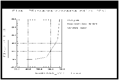
You may wish to check the linearity of the device response by viewing the i_vs_va plot, which displays the device current vs voltage on a log scale. The more (log) linear the response, the closer the diode is to being ideal. The illustration gives an example. |
Figure 101 Example Log Scale Plot of Current vs Voltage
|
|
| 13 |
When you are done, close the plots. |
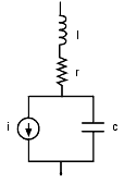
Measuring and Extracting Parasitic R and L Values
This procedure measures S-parameters vs frequency, with the diode forward-biased and a fixed value of forward conducting current. The program calculates the intrinsic parasitic resistance (r) and inductance (l) values from the measured data. The illustration below is a simplified schematic representation of the intrinsic r and l values. In calculating r and l the program takes into account the extrinsic parasitic capacitance, inductance, and resistance values entered in the Parameters table at the beginning of the procedure.
Figure 102 Simplified Schematic Diagram of Intrinsic r and l
|
|
|
Note
|
|
|
|
|
Make sure you have calibrated the network analyzer before you begin this procedure. Refer to the instructions earlier in this chapter.
|
|
Defining the Instrument States
Perform the same Instrument Options procedure you did for the s_vs_f measurement. Pay particular attention to the notes listed in that procedure. The instrument states need to be set independently for each setup.
Setting the parasitics Input Values
Most of the input parameters for this measurement are factory preset and should not be changed. The current values are based on values you set in the model variable table at the beginning of the procedure. The other inputs are necessary to set up the required device measurement configuration.
| 1 |
Select the parasitics setup. |
| 2 |
Set the ia voltage Compliance to around the same value as the a Stop value used in the i_vs_v DC preverification, or slightly higher. |
| 3 |
The ia Sweep Type is set to CONstant with a Value of IFwd to drive the diode with a constant maximum forward conducting current. |
| 4 |
The vc Sweep Type is set to CONstant with a value of 0.000, to ground the cathode. |
| 5 |
The vc Compliance value of 1.1*IFwd limits the current to a value 10% above IFwd to prevent damage to the device. |
| 6 |
The freq inputs set the network analyzer for a linear sweep of the calibrated frequency range. Set the freq Start and Stop values to correspond with the frequency range of your calibration. |
| 7 |
Set the # of Points to correspond with the calibration. |
Measuring, Plotting, and Extracting
| 1 |
Select Plots > Display All. |
| 2 |
Select Measure/Simulate > Measure. The program automatically calculates the r and l values vs frequency from the measured data and enters them in a file named Para.data. (The z transform is automatically executed after the measurement.) |
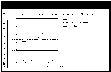
- The plots display the parasitic r and l as a function of frequency. The resistance data displayed is the real part of the measured impedance z.m. The inductance data is the imaginary part of z.m divided by 2
 f. f.
- The parasitics will be recalculated later at the frequency of extraction only.
The Main Data Acquisition
This is the main measurement procedure that takes the data from which the model will be generated. The procedure measures S-parameters over a calibrated microwave frequency range, across a range of bias voltages. It takes adaptive measurements, densely spaced in the most nonlinear regions such as at the onset of breakdown and the knee of the forward conducting curve, and less densely spaced in the reverse-bias region (except where the capacitance data changes rapidly). The number of data points measured depends on the nonlinear behavior of the device and on the measurement conditions you set up.
Preparing
Some knowledge of the device characteristics is needed in order to input valid parameters. Follow the steps below to input appropriate values for your device. Do not exceed maximum allowable values. (If a data sheet is available for the device, refer to it for specifications and compliances.)
Defining the Instrument States
The instrument states for the data acquisition are set in the dc_bias and ac_bias setups.
|
Caution
|
|
|
|
|
Do not change the inputs in the dc_bias or ac_bias setups. Their function is not the same as in the other setups. They contain factory-set information essential to the program, and they must not be changed.
|
|
| 1 |
Select the dc_bias setup. |
| 2 |
Select the Instrument Options tab to display the DC source/monitor instrument states. |
| 3 |
Set the Agilent 4142 instrument state the same as for the i_vs_v DC preverification and the ideality measurement. |
| 4 |
Select the ac_bias setup. |
| 5 |
Set the instrument states the same as for the s_vs_f preverification and the parasitics measurement (otherwise the calibration will be invalid). |
Defining the Voltages and Step Sizes for the Measurement
| 1 |
Select the create_mdl setup. |
| 2 |
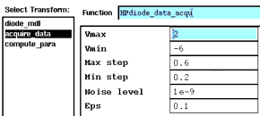
Select Extract/Optimize > acquire_data. The table illustrated below is displayed. |
Figure 103 Opened acquire_data Transform in create_mdl Setup
|
|
| 3 |
Edit the variable values in the transform by entering values appropriate for your own device. |
| 4 |
For the value of Vmax, enter the maximum allowable forward voltage. |
| 5 |
Enter a value for Vmin that corresponds to the reverse breakdown voltage. |
| 6 |
Enter a value you choose for Max step. This defines the measurement step size for regions where you expect the data to be relatively linear and measurements to be more widely spaced. |
| 7 |
Enter a value you choose for Min step. This defines the step size for densely-spaced measurements where the data is most nonlinear. |
| 8 |
Enter a value for Noise level. This is the current threshold value below which the automatic step-size algorithm is not used. Set a value below which you do not need closely-spaced measurements, as measured currents below this value are sampled at the maximum step size. |
| 9 |
Enter a value for Eps (epsilon). Epsilon is used to predict the next point to be measured and thus control automatic data acquisition step size. Increasing the value of epsilon decreases the sensitivity of the automatic data acquisition. Epsilon should generally be between 0.1 and 0.3; the default value is 0.1. |
| 10 |
If you wish to save these transform values for use with similar devices, select File > Save As. Then select the File Type Transform, type in a filename that conforms to UNIX requirements, and select OK. The file is saved with the suffix .xfm for transform. |
The create_mdl Inputs
Don't change the inputs. The create_mdl setup, like the other setups, includes an input configuration list. However, the function served by this list is not the same as in the other setups. It is factory-set internal information used by the program, and is essential to its function.
Performing the Data Acquisition Measurement
This procedure performs the measurement you defined. Once you initiate the transform, the data acquisition procedure takes approximately 10 to 20 minutes. The data acquisition rate is approximately 10 points per minute. The number of data points measured depends on the nonlinear behavior of the device and on the measurement conditions you set up.
Measuring and Extracting
| 1 |
In the create_mdl setup select the Extract/Optimize tab. |
| 2 |
Select acquire_data > Execute. During the data acquisition process, a running message in the UNIX window indicates the approximate percentage of completion. |
|
Caution
|
|
|
|
|
Do not perform data acquisition more than once. This will write over the existing data, and will use more time and memory.
|
|
| 3 |
If you do attempt to perform data acquisition after the measurement has already been done, a message will ask you DO YOU WISH TO OVERRIDE?. You then have several choices: If you do not need the data in the current file you can select Return or OK to overwrite it. Or you can abort your new measurement by selecting Cancel. Or if you wish to save the measured data and perform another data acquisition, go to the UNIX window, change directories if necessary, and rename the file Measured.data with another appropriate name, then continue with the data acquisition. |
| 4 |
Ignore this message if it occurs: CAUTION: CALSET X STATE MAY BE INVALID. |
| 5 |
When the process is complete, a message similar to the following is displayed in the UNIX window: |
- INITIAL Extraction Results
Pts_num = 66.00
Done!
- The numbers are part of the internal function of the program, and irrelevant in user interaction with the program. They are associated with the number of points in the measurement.
Plotting the Measured Data
The plots in the create_mdl setup provide graphical outputs of the data acquisition and model generation. For hardcopy output, black and white can be reversed for faster printing and easier reading on paper, as explained in the procedure.
If you wish to plot data from a previously stored data set, you will need to perform the steps explained under To Plot an Earlier Measurement. Otherwise, follow these steps:
Viewing and Printing the Plots
| 1 |
From the Plots tab, select the plot of your choice, and Display Plot. |
| 2 |
You can augment the annotation of a plot by specifying header and footer labels you wish to print with the data. However, it is essential not to change the Y data input fields. |
| 3 |
To change a plot's annotation, go to the Header or Footer lines in the plot definition. You can type a label of your choice in the header or footer input field (right side of the definition table). Then select Options > Update Annotation, and your label is added to the plot. |
|
Note
|
|
|
|
|
Changing the Y Data n input fields can cause anomalies in the measurement and modeling results.
|
|
| 4 |
If you wish to exchange the black and white in a plot for better hardcopy quality, select Options from the plot menu, and Exchange Blk Wht from the pull-down menu. You can also change from colored traces to all black by selecting Options > Color. This is particularly useful if one of the traces is a light color such as yellow, which may not show well against a white background. |
| 5 |
To get a hardcopy of a plot, from the plot menu select File > Print Setup. Enter the name of a printer and make any other changes to the printer/plotter setup you wish, then select OK. Select File > Print. |
To Plot an Earlier Measurement
If you wish to view data from a previously stored Agilent Root diode measurement, you will need to perform these extra steps to bring the data into this model and display the plots.
| 1 |
From the IC-CAP main menu select File > Change Directory. Type in the pathname of the file where your data is stored, and select OK. |
| 2 |
Select the create_mdl setup and select the Plots tab. |
| 3 |
Select the plot of your choice, and Display Plot. (The displayed plot window will be blank and an error message will be displayed.) Ignore the error message and click OK.) Now select Display Plot again, and the plotted data will be properly displayed. (The first time you selected Display Plot, an internal function re-initialized the data from the changed directory.) |
Generating the Model
This procedure calculates the model parameters from the measured data, and generates a corresponding model for the device.
If you are generating a model from a previously stored data set, perform the steps listed later in this procedure under "To Generate a Model Using Data from an Earlier Measurement." Otherwise, follow these steps:
Defining the Extraction Frequency
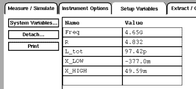
The model is extracted at a single frequency, which should be approximately the frequency at which the device will be used. It must be one of the measured points from the calibrated frequency list. To determine a frequency for the extraction, use a calibrated measurement point equal to the start frequency plus an integer multiple of the step size. For example:
- 200 MHz (start freq) + 1 · 4.45 GHz (step size) = 4.65 GHz
| 1 |
In the create_mdl setup select the Setup Variables tab. The variables table illustrated is displayed. |
Figure 104 Variable Table of the create_mdl Setup
|
|
| 2 |
Manually change the value of Freq to your chosen extraction frequency. |
Computing the Parasitics at the Extraction Frequency
| 1 |
Select Extract/Optimize > compute_para > Execute. This calculates the parasitic r and l values at the extraction frequency and enters them in the create_mdl variables table, in place of the average value of the parasitics over the total measured frequency range. |
Scaling the i Plot Before Generating the Model
Sometimes excessive noise may be present in the IV characteristics near zero, although this is not generally visible with standard scaling. To prevent the model generation process from interpolating data points in this noisy region, the model can smoothly join the data outside this region and connect it across the noisy region.
The following steps use the measured data in the i plot to determine if there is excess noise near zero, and to curve-fit the measured data if necessary.
| 1 |
Select Plots > i > Display Plot. |
| 2 |
To obtain a closer view of the measured data around the knee of the forward conducting current curve, click trace points to the left and right of zero to redefine the plot range. Then in the plot menu select Options > Rescale to expand the plot to the new range. |
| 3 |
Perform the last step repeatedly until you can see if there is low-level noise on the trace. |
- If the current appears smooth even at expanded resolution, go to Executing the Transform.
Figure 105 i Plot Expanded to Show Data Near Zero
|
|
- If the current appears noisy at expanded resolution, use the X-low/X-high function for curve-fitting, as follows:
| |
• |
Click the mouse at the left and right boundary points of the noisy portion of the trace, to make a box on the trace. |
| |
• |
From the plot menu select Options > Copy to Variables. This sets the X-LOW and X-HIGH values in the create_mdl setup variable table to the boundary points you selected. It also sets the values for LowBound V and HighBound V in the diode_mdl transform. |
| |
• |
Note that the value for X-low should be slightly negative and for X-high should be slightly positive. An error message will be displayed if the values are inappropriate. |
| |
• |
Now when the model is generated, the noisy data will be averaged over the X-low/X-high range you defined. |
Executing the Transform
| 1 |
Select the Extract/Optimize tab. |
| 2 |
Select diode_mdl > Execute to start generating the model for the device under test. |
| 3 |
A dialog box asks you for an MDS file name. The standard file generated by the model for interface with MDS is named diode.mds. If you want to retain this filename select OK or press Enter. Otherwise change the name to a new filename that associates this model with the device, retaining the suffix .mds for compatibility with MDS. |
|
Note
|
|
|
|
|
If you plan to do a verification, retain the filename diode.mds for now, as the verification process requires this filename. You will have another opportunity to change the filename after the verification process.
|
|
| 4 |
A Done! message in the UNIX window indicates when the model generation is complete. |
Generating a Model from Previously Measured Data
If you wish to generate a model from a previously stored measurement, you will need to perform this additional step to bring the measured data into this model.
| 1 |
From the IC-CAP main menu select File > Change Directory. Type in the pathname of the file where your data is stored, and press Return. |
| 2 |
Now perform the standard procedure, "Generating the Model," described above. |
Plotting the Generated Data
| 1 |
To view a specific plot select the plot and Display Plot. The c plot displays the high-frequency intrinsic capacitance as a function of voltage. The following figure shows capacitance data for an example device. The response is properly flat below pinch-off for this FET-like diode, with more points taken where the capacitance changes faster. The data is extrapolated in the forward region where forward bias capacitance is not extractable. |
Figure 106 Example Capacitance Data
|
|
|
Note
|
|
|
|
|
Capacitance characteristics of different diodes may be extremely different.
|
|
| 2 |
The compare_i plot displays the agreement between the modeled and measured current. When agreement is good, it may be difficult to distinguish the extracted data (yellow trace) from the measured data (red trace). To expand the trace resolution, from the plot menu select Options > Rescale. The data illustrated in the following figure shows good agreement even with expanded resolution. |
Figure 107 Example compare_i Data
|
|
Other Outputs of the Model Generation Process
The model generation process results in a number of different output files to be used for different purposes. These include the model file for MDS interface, data on various modeled parameters, measured device data, and files for internal use by the program.
Some files have default filenames assigned by the program. Others may be files you created during the procedure to save device-specific information.
|
Caution
|
|
|
|
|
In general, the files should NOT be modified, because changing them can cause problems that may invalidate the model. It is also important that you do not change the names of files created by the model generator, with the exception of diode.mds.
|
|
Following is a list of some files that will be or may be created during the modeling process:
| • |
icplotnotes. This is the only file you can safely edit or add to. The program appends it as a label to any graphical outputs, to identify the device. It includes a device ID string and any additional information you choose to add to graphs when they are plotted. |
| • |
icplotnumbers. This is an internal file used by the program to generate a graphical interface. It is related to the Pts_num message that appears in the UNIX window at the end of the data acquisition. While the Pts_num parameter is irrelevant to user interaction with the program, it is essential to its function, and must appear on the screen. Do not change this file. |
| • |
Measured.data. This is the raw measured S-parameter data as a function of bias and frequency, produced by the create_mdl data acquisition process. |
| • |
Para.data. This is the S-parameter vs frequency data at forward bias, used by the program to calculate parasitic resistance and inductance values. |
| • |
Diode.data. This file is used by the program in plotting nonlinear functions. Do not change this file. |
| • |
Diode.mds. This is the model file used by the Agilent RF and Microwave Design System (MDS) in a circuit simulation. It is also used in verifying the model, and needs to retain the name Diode.mds in the verification process in order to maintain the MNS simulator link. However, since every Agilent Root diode model initially has this name, you change the name to identify the device, either when you execute the transform to generate the model (if you are not performing a verification), or at a later time as described at the end of this chapter. |
| • |
dc_test.set (or some other name designated by you). If you decided to save it, this is the measured DC data generated in the DC preverification procedure. |
| • |
spar_test.set (or some other name designated by you). If you decided to save it, this is the measured S-parameter data generated in the S-parameter (AC) preverification. |
Verifying the Model DC Data
This procedure verifies the model DC data against the DC data measured in the i_vs_v setup, using the MNS simulator link.
|
Note
|
|
|
|
|
The simulator used must be MNS. If the SIMULATOR in the model variable table is set to another value, change it to mns.
The name of the model file must be Diode.mds for purposes of verification, to maintain the MNS simulator link.
|
|
| 1 |
Select the i_vs_v setup. Make sure the output Type is set to B for both measured and simulated data. |
| 2 |
From the Plots tab, select the i_v plot, and Display Plot. |
| 3 |
Select Measure/Simulate > Simulate. |
| 4 |
Check that the simulated data (dotted line) on the plot is in good agreement with the measured data. |
Verifying the Model S-Parameter Data
This procedure verifies the model S-parameter data against the S-parameter data measured in the s_vs_f setup, using the MNS simulator link.
|
Note
|
|
|
|
|
The simulator used must be MNS. If SIMULATOR in the model variable table is set to another value, change it to mns.
The name of the model file must be Diode.mds for the purposes of verification, to maintain the MNS simulator link.
|
|
| 1 |
Select the s_vs_f setup. Make sure the output Type is set to B. |
| 2 |
Select Plots > sp > Display Plot. |
| 3 |
Select Measure/Simulate > Simulate. |
| 4 |
Check that the simulated data (dotted lines) on the plot is in good agreement with the measured data. |
Generating a Model at Another Frequency
You may wish to generate a model at a different frequency, which must be another measured point from the calibrated frequency list (see Defining the Extraction Frequency). (During the data acquisition, data was taken at each of the calibrated frequencies in the frequency list.) If so, follow these steps:
| 1 |
If you are satisfied with the model you have just generated, copy the file Diode.mds to another filename. (Be sure to use a different name for the new model than you used for the first one.) |
| 2 |
Select the create_mdl setup. |
| 3 |
Select the Setup Variables tab to open the create_mdl variable table. |
| 4 |
Change the value of Freq to the new calibrated frequency of your choice. |
| 5 |
Select Extract/Optimize > compute_para > Execute to calculate the parasitic r and l values at the new extraction frequency. |
| 6 |
Select diode_mdl > Execute to start generating the new model. Unless you wish to perform a verification afterwards, enter another filename, possibly one that includes the new extraction frequency. |
| 7 |
When the Done! message appears in the UNIX window, observe the plots. |
| 8 |
If you wish, verify the model against the measured DC and S-parameter data using the previous procedures. |
Storing Your Model and Interfacing with MDS
Once you have developed your device model, you can store it in a file for future use. You can use it for circuit simulation in the Agilent RF and Microwave Design System, inserting it into circuits under design to emulate the characteristics of your device. It can be used to represent any device with the same geometry from the same process, or scaled to represent a different-sized device. It will predict the gain, power, gain compression, and harmonics performance of the device as a component in circuits you design using MDS. It will predict large-signal device operation over a range of bias points and loading conditions.
The file generated by the modeling process for interface with MDS is called Diode.mds. You need to change the name to one that will identify the device under test, since every Agilent Root diode model file is initially named Diode.mds.
If you chose not to perform a verification, you may have already changed the filename using the dialog box presented before the diode_mdl transform. If not, you can change the filename now in UNIX and store the file as follows:
Storing the Model
| 1 |
Use the UNIX directory you created at the beginning of the procedure, when you first opened the model file. |
| 2 |
From the IC-CAP Main window select File > Save As. |
| 3 |
A dialog box is displayed. Select the File Type (.mdl for a complete model) by clicking on the corresponding radio button. |
| 4 |
Select a new filename that associates this model with the device. |
| 5 |
Use the UNIX cp command to copy the file Diode.mds to the new filename, including the pathname of the designated directory. Select OK. |
This completes the example Agilent Root diode measurement and model generation procedure. For an explanation of how to use IC-CAP model data in MDS, refer to Appendix D, "Using IC-CAP Data with MDS."
|