Using the Agilent Root MOS Model
This chapter provides an example procedure that takes you step-by-step through a measurement and model generation of an NMOS device. Values you use in generating your own device model will depend on the particular characteristics of your device: use its data sheet (if available) as a reference.
This example is provided as a starting point. It is a straightforward procedure that uses only a subset of IC-CAP's total capabilities. The complete procedure documented gives all the steps necessary to configure IC-CAP with the parameters for preverification measurements, parasitic extractions, and the main data acquisition. Once a model has been developed for a particular device type, the built-in scaling feature allows you to apply it to any device with the same process and a different total gate width and/or number of fingers. The modeling procedure then becomes more simple, and can be accomplished in a few easy steps.
|
Note
|
|
|
|
|
Although you will modify the variable values in factory default files during this procedure, do not under any circumstances change the names of any variables or setups. These names are used by the software in the data acquisition and model generation process.
|
|
|
Note
|
|
|
|
|
The example procedure measures the MOSFET under test in a common-source configuration.
|
|
The example procedure gives detailed instructions on how to:
| • |
Initialize device parameters. |
| • |
Measure and extract the system measurement port series resistances. |
| • |
Make a DC measurement to preverify device DC performance. |
| • |
Calibrate the network analyzer for both swept and CW measurements. |
| • |
Make an S-parameter measurement to preverify device performance at high frequencies. |
| • |
Measure and extract the device parasitic resistances. |
| • |
Set up and initiate the main data acquisition. Plot the measured data. |
| • |
Set up and initiate the model generation. Plot the calculated state functions. |
| • |
Verify the model against measured data. |
| • |
Store the data and model files for circuit simulation in Agilent MDS. |
|
Note
|
|
|
|
|
Measurement parameters and measured data are specific to individual devices. Information and data are provided here as examples and guidelines, and are not intended to represent the only correct results.
|
|
The procedure provides guidelines on setting values to measure your device. However, the values you use will be based on your knowledge of your device and on information in its data sheet, as well as on the guidelines presented here: they may or may not correspond with the example values.
The illustrations of plotted data are provided as visual examples of possible results. They are not intended to represent a single device, nor do they necessarily correspond with the values given in the procedure. The plots can be used to check the reasonableness of your own data, which should appear similar in shape but not necessarily coincident in values.
The DUT and Setups
The Model window is the central access point for all the procedures in the measurement and model generation process. The Model window includes the DUT/Setup panel and the file tabs to access the Model Parameters table, the model variable table, and other needed IC-CAP features.
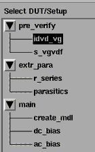
The illustration shows the DUT/Setup panel for the model generator file HPRootMos.mdl. The DUTs (for example pre_verify) indicated by the inverted triangles are groupings of similar measurement setups used to make related measurements or extract related model parameters. The setups (for example idvd_vg) contain the information used to define the inputs and outputs for each measurement and extraction, as well as the measurement hardware configurations and the transforms and plots associated with each setup.
Figure 77 Agilent Root MOSFET DUT/Setup Panel
|
|
Initializing Device Parameters
You begin the procedure by giving the device an identifying name, and entering the number of fingers and gate width. For this you use the init_parameters macro. When this macro is executed, it also initializes internal program functions that are essential in the model generation process, and it provides annotations for the data plots. (IC-CAP macros are used to combine or simplify operations.)
| 1 |
Click the Macros tab to display the macro names. |
| 2 |
From the Select Macro list, select init_parameters, and Execute. |
| 3 |
In the dialog box that appears, enter a name to identify the device under test, then click OK or press Return. |
| 4 |
In the next dialog box, enter the number of gate fingers. |
| 5 |
Next enter the gate width in meters. |
| 6 |
The next dialog box prompts you for a directory name. Click OK to store the model files in the directory shown, enter the name of another existing directory. Click OK or press Return. |
| 7 |
The macro is executed, and the values you selected are entered in the model variable table. You can open the table by clicking on the Model Variables tab. |
|
Note
|
|
|
|
|
Do not edit the init_parameters macro. The macro includes executable code; modifying it can cause problems in the program.
|
|
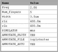
Setting the Extraction Frequency
You use the model variable table to set the frequency at which the model will be generated. To edit the variable table, move the mouse pointer to the appropriate variable value, click left, and move the pointer over the old information to highlight it. Then type in the new value over the old.
Figure 78 Model Variable Table
|
|
| 1 |
Enter the CW frequency you intend to use for the data acquisition and model generation. This must be the same as the frequency of the network analyzer CW calibration you will perform before doing any S-parameter measurements. Refer to the explanation under Calibrating the Network Analyzer, which explains how to perform a CW calibration and how to decide the CW frequency. |
| 2 |
Make sure the Value listed for SIMULATOR in the model variable table is mns, to ensure that the mns link is in place to allow verification of the model in IC-CAP. |
| 3 |
Do not change the other values in the table at this time. |
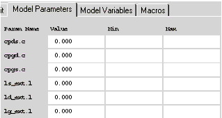
Values in the Parameters Table
The illustration shows the Model Parameters table, with the initial values for the extrinsic parasitic capacitances and inductances. The table is presented here so that you can enter values for these extrinsic parasitics based on your knowledge of the device, or on estimates, or on measurements of the open fixture. In addition, you can set limits by entering minimum and maximum values for each parameter. Parameter values that are outside their limits are clamped to their minimum or maximum values.
Figure 79 Model Parameters Table
|
|
To access the Parameters table, click on the Model Parameters tab.
To change a value in the Parameters table, move the mouse pointer over the current entry and click left to highlight it, then type in a new value.
The default for all the c values is 0.000. A reasonable capacitance value to enter for a pad on a wafer might be 50 fF.
The l_ext.l values are the bond inductances for the three terminals. The default value for all three is 0.000. If you know or can estimate the bond inductances for your device based on wire length or grid size, enter appropriate values.
Extracting the Measurement Port Series Resistances
This procedure need be performed only following initial installation of the system or if changes are made in the system hardware.
The procedure measures a short circuit at the normal device measurement interface plane. IC-CAP controls the DC source/monitor to force a gate current and monitor the gate voltage. The primary measurement is at port 1, and the port 2 measurement is synchronized to the port 1 measurement. You set the measurement parameters by defining the instrument state and the DC input values, as explained in the next pages.
The software calculates the series resistances from the outputs of the bias networks to the inputs of the device under test. The resistance values are then incorporated into the model file, and their effects are removed from the device response during the modeling process. The default port resistance for both port 1 and port 2 is 0 . .
Note that the first part of the procedure differs for probe station and in-fixture measurements.
Setting Up for the Measurement
| 1 |
If you are using a probe station, position an impedance standard substrate (ISS) on the chuck. Place both the port 1 and port 2 probes on a short circuit standard. |
| 2 |
If you are using a fixture, insert the short from the in-fixture calibration kit. |
| 3 |
From the DUT/Setup panel select the r_series setup. |
Defining the DC Source/Monitor Instrument State
Follow the steps described in the appropriate chapter shown next:
Set Integ Time to M (medium). Then return to this chapter and continue.
Setting the r_series Inputs
Use the following guidelines to set the ig and id inputs (most will not need to be changed from the default settings):
Table 23 For the ig input
|
|
Mode
|
I
|
To Node
|
G (gate)
|
From Node
|
GROUND
|
Compliance
|
as high as 5 to 10V, because the device is not yet connected
|
Start, Stop
|
values that define a current range within the limits of the bias network
|
# of Points
|
a value sufficient to make several measurements across the current range
|
The Step Size will be set automatically
|
| • |
The Unit name must match the name of the SMU connected to the device gate (probably VG). This is also the SMU unit name set in the hardware window. Refer to the appropriate chapter as follows: |
| • |
With a current input, compliance refers to voltage. |
|
Caution
|
|
|
|
|
The bias networks can be destroyed if IC-CAP measurement current values are set too high! Be sure you know the maximum current ratings of your bias networks, and do not set current values beyond these limits. (The standard bias networks for the Agilent 85122A and 85123A parameter extraction test systems are rated at 0.5 amp.)
|
|
Table 24 For the id input
|
|
Mode
|
I
|
To Node
|
D (drain)
|
From Node
|
GROUND
|
Unit
|
VD
|
Compliance
|
the same as for ig
|
Sweep Type
|
SYNC
|
Ratio
|
1.000, so that the id sweep is synchronized to the ig sweep
|
Offset
|
0.0
|
Master Sweep
|
ig, so that the id sweep is synchronized to the ig sweep
|
| • |
The Outputs are factory set, and should not be changed. |
Measuring and Extracting the Port Series Resistance Values
| 1 |
Under Measure/Simulate select Measure. |
| 2 |
When the measurement is complete, the Measuring light on the DC source/monitor goes out and the IC-CAP wristwatch icon goes away. |
| 3 |
Select the Extract/Optimize tab. |
| 4 |
Select compute_rseries > Execute. The transform calculates the port series resistances from the measured data and enters the values into the model variable table as r1s and r2s. |
Installing the Device
|
Caution
|
|
|
|
|
Ground yourself with an antistatic wrist strap to reduce the chance of electrostatic discharge. (Note that the Agilent 85122 or 85123 system work surface is coated with antistatic material and is connected to chassis ground, therefore a static mat is not required.)
|
|
Install the device carefully on the probe chuck or in the fixture. Be sure to handle the device as little as possible, to avoid damaging it. Once the device is in place, avoid bumping the test station.
|
Caution
|
|
|
|
|
Remove any high-intensity light sources such as microscope light before taking a measurement. One simple method of blocking light is to place an opaque box on the fixture directly above the device.
|
|
Preverifying the Device DC Data
This procedure uses the idvd_vg setup to measure drain current and gate current with respect to drain voltage, at several values of gate voltage. The drain voltage is swept from 0V to the upper limit of its normal operating range. This is an opportunity to take a first look at the device performance and explore its characteristics. This also lets you select the most appropriate measurement range for the main data acquisition and other measurements.
In addition, this is a quick way to verify that the device DC characteristics are good, before starting a complete data acquisition and modeling generation. The data from this measurement can also be used for later comparison with data predicted by the generated model. It is not necessary to do the preverification measurement every time you perform a model generation, especially if you are using a data sheet.
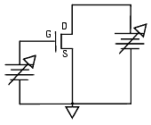
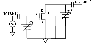
Device Configuration: The input values you set in this procedure configure the device as shown in the following figure.
Figure 80 MOSFET Bias Configuration for DC Preverification
|
|
Defining the DC Source/Monitor Instrument State
Follow the same process you used in the r_series measurement. Use the same settings.
Then return to this chapter and continue.
Setting the idvd_vg Inputs
This procedure defines the input signals to be applied to the device under test for the DC preverification measurement.
The actual settings you use will be dependent on the compliance limits for both the device and the SMUs/bias networks, and on the range of measurements you wish to take. Since this measurement is intended only to preverify the device, the values can be quite conservative and need not stress the device to the boundaries of its performance.
If you are measuring a series of devices of the same type and have already set the input parameters, go directly to Measuring and Plotting. Otherwise, select the idvd_vg setup use the following settings as a guideline:
Table 25 For the vd input
|
|
Mode
|
V
|
Compliance
|
no greater than the maximum breakdown current value for the device
|
Sweep Type
|
LIN, to provide a linear voltage sweep from start to stop voltage values
|
Start
|
0.0
|
Stop
|
at or below the upper limit of the device's normal operating range
|
# of Points
|
sufficient to clearly display the measurement results
|
The Step Size will be set automatically
|
Table 26 For the vg input
|
|
Mode
|
V
|
Compliance
|
no greater than the maximum allowable gate current value.
|
Sweep Type
|
LIN, to provide a linear voltage sweep from start to stop voltage values
|
Start, Stop, # of Points
|
such that three to five values (points) will be measured, in a range from approximately Vgs=Vthreshold to Vgs=3 or 4V. Set Start to a value close to Vthreshold, but not so close that the curve will be difficult to discern.
|
The Step Size will be set automatically
|
|
Note
|
|
|
|
|
The vd and vg ranges apply to an NMOS device. Recognize that for a PMOS device both vd Start and vg Start will be negative, and Stop will be 0.000.
|
|
| • |
The Unit names must conform to the names you set in the hardware window when you configured IC-CAP to recognize the system hardware (probably VD and VG). They must also correspond with the actual SMU (source/monitor unit) connections from the Agilent 4142. Since the device source terminal is grounded, only the drain and gate inputs need to be set. |
| • |
You provide compliance values to limit SMU output voltage or current and thus prevent damage to the device under test, as well as to the SMUs, bias networks, and probes if used. With a voltage input, compliance refers to current. |
| • |
The Outputs are factory set, and should not be changed. |
Measuring and Plotting
This procedure triggers the DC source/monitor measurement and monitors the results.
|
Note
|
|
|
|
|
Before making the DC measurement, manually put the network analyzer in hold sweep mode by pressing STIMULUS > MENU > MORE > HOLD on an Agilent 8510, or MENU > TRIGGER MENU > HOLD on an Agilent 8753.
Be sure to keep a UNIX window open so that you will see any compliance error that may be reported by the DC source/monitor.
|
|
| 1 |
From the Plots tab, select Display All (to the left of the setup window). Two plots are displayed. |
| 2 |
Select the Measure/Simulate tab, then select Measure. When the measurement is complete, the Measuring light on the DC source/monitor goes out, the IC-CAP wristwatch icon disappears, and the measured data is displayed in the plot window. |
| 3 |
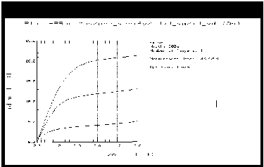
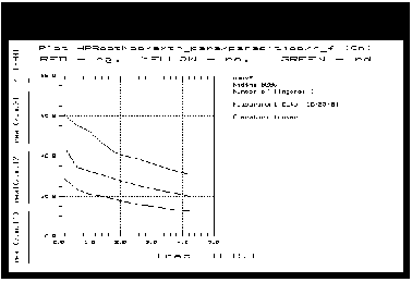
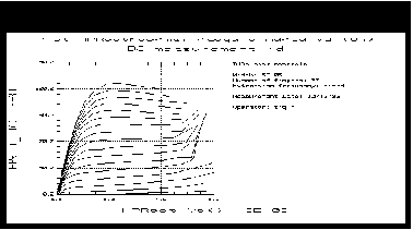
Check the id_vd plot. The data displayed should resemble that shown in the following figure, with the lowest curve close to the X-axis to show the threshold characteristics. If the data indicates the device is not operating in its normal range, go back to the inputs and change the gate voltage values. (If more than one curve is low, change vg Start to a higher value. Or if all the curves are high, change vg Start to a lower value.) Then select Measure again. |
Figure 81 Example Measured pre_verify id_vd Data
|
|
| 4 |
If the measured data looks wrong for your device, check the probe contacts, the bias connections, and the measuring instruments. Make sure the device is oriented properly, with the right ports connected to the right terminals. If none of these resolves the problem, the device may be defective. For example, if all the curves are superimposed, the gate may be shorted. |
| 5 |
To save the measured data for later comparison with data predicted by the extracted model, choose File > Save As and a filename with the suffix .set (for example dc_test.set). Then click OK. |
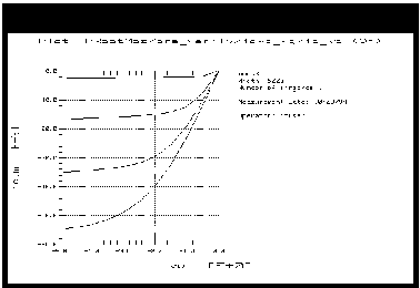
| 6 |
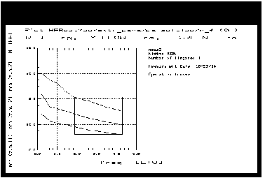
The following figure illustrates a typical id_vd plot for a PMOS device. |
Figure 82 Example Measured id_vd Data for a PMOS Device
|
|
Calibrating the Network Analyzer
It is important to calibrate the network analyzer before you perform any S-parameter measurements. Good calibration of the network analyzer is critical to a good measurement and model generation.
The Agilent Root MOS measurement procedures require two network analyzer calibrations: a swept broadband cal and a CW cal. The broadband cal is used for the S-parameter preverification and parasitics measurements. The CW cal is used for the main data acquisition.
For a system with an Agilent 8510 network analyzer, this procedure uses the frequency list cal mode for both the broadband and CW calibrations. The two calibrations can be done with only one set of standards measurements, by making the CW cal a subset of the broadband cal. For a system with an Agilent 8753 or 8720 network analyzer, two separate calibrations must be performed.
Frequency list calibration procedures for an Agilent 8510-based system and an Agilent 8753-based system are provided in the next few pages. A CW calibration subset procedure for an Agilent 8510-based system is also provided.
Calibration for an Agilent 8753-Based System
Although the Agilent 8753 has frequency list capability, IC-CAP does not support the subset calibration technique used in an Agilent 8510 system. Therefore it is necessary to perform two separate calibrations for an Agilent 8753- or 8720-based system: one frequency list calibration and one CW calibration. A separate set of standards measurements must be made for each calibration.
Frequency List Mode
Frequency list lets you define an arbitrary list of frequencies in one or more segments. During the measurement sweep the synthesizer is phase-locked at each frequency point, as in the stepped-sweep mode. The advantage of frequency list mode for use in a table-based model such as this is that it lets you define a smaller number of measurement points than for a step or ramp frequency cal. This reduces the total measurement time. A # of Points of 11 provides adequate measurement resolution as well as a quite fast total measurement time.
For the purpose of this model you will define two frequency segments in the list, a swept broadband segment and a CW segment. Set the broadband frequency list segment range at least as wide as the operating range of the device.
Set the CW frequency segment to the frequency you intend to use for the data acquisition, the same frequency you set in the model variable table at the beginning of this procedure. This frequency should be above 200 MHz to eliminate the effects of test set coupler roll-off at low frequencies, and low enough to eliminate bond inductances and other parasitic inductance considerations.
Based on the broadband cal, use a calibrated measurement point equal to the start frequency plus an integer multiple of the step size. An example frequency might be 600 MHz.
200 MHz (start freq) + 1 · 400 MHz (step size) = 600 MHz
Frequency List Calibration for an Agilent 8510-Based System
If you are using an Agilent 8510-based system, follow the steps below.
| 1 |
On the network analyzer press PRESET. |
| 2 |
To define a linear frequency list, on the network analyzer press STIMULUS > MENU > MORE > EDIT LIST > ADD. A default frequency list segment is presented. |
| 3 |
To change the segment to your chosen frequency range press SEGMENT: START, and use the numerical keypad to set the start frequency, ending with one of the terminator keys (such as M/ ) at the right of the keypad. Similarly, press STOP and set the stop frequency. ) at the right of the keypad. Similarly, press STOP and set the stop frequency. |
|
Note
|
|
|
|
|
Use the SEGMENT: START and STOP softkeys, not the START and STOP hardkeys in the STIMULUS area of the front panel.
|
|
| 4 |
Press SEGMENT: NUMBER of POINTS, and enter the number of frequency points to be measured across the range. Keep in mind that the fewer the number of points, the less time the measurements take. |
| 5 |
Press DONE to return to the frequency list menu. The segment you just defined is listed on the screen. |
| 6 |
Press DONE to return to the main stimulus menu. Press FREQUENCY LIST to activate the frequency list mode. |
| 7 |
Press PRIOR MENU > MORE > CONTINUAL to set a continual stimulus sweep. |
| 8 |
Press PRIOR MENU > POWER MENU, and set the desired power level. In setting the source power and attenuation, take care that the power level will not be excessive at the device input. Also consider the gain of the device, and set a power level that will not saturate the input port samplers of the analyzer. If the power level at the sampler goes above  -8 dBm, an IF OVERLOAD error message is displayed and you will need to reduce the source output power. The default network analyzer power level is 0 dBm. -8 dBm, an IF OVERLOAD error message is displayed and you will need to reduce the source output power. The default network analyzer power level is 0 dBm. |
| 9 |
For a device with power drop-off at higher frequencies, you may wish to set a power slope using the stimulus menus. An appropriate power slope would be in the region of 2-3 dB/GHz. |
| 10 |
Press RESPONSE MENU > AVERAGING ON/restart, and enter an averaging factor high enough to reduce trace noise and increase dynamic range as appropriate for your device measurements. Although the default is 256, you may wish to use an averaging factor as low as 16 to reduce overall measurement time. |
| 11 |
If the cal kit constants for your calibration kit are not loaded into the network analyzer, load them from disc now by pressing DISC > LOAD and specifying the data type and file name. |
| 13 |
Press CAL > CAL1 or CAL2 (depending on your cal kit), and perform a two-port calibration, measuring each of the standard devices in turn and pressing the softkeys as each measurement is complete. |
| 14 |
At the end of the calibration sequence, the cal set numbers are listed in the softkey menu. Press CAL SET #1 to store the calibration in cal set #1. (Or use another available cal set.) |
CW Calibration Subset for an Agilent 8510-Based System
| 1 |
To create a CW frequency subset of the broadband frequency list calibration, press CAL > CORRECTION ON > CAL SET 1 (this turns on the broadband cal you just completed), then MORE > MODIFY CAL SET > FREQUENCY SUBSET. Use the SUBSET: START and SUBSET: STOP softkeys in the SUBSET menu (NOT the front panel keys) to set both start and stop to the same frequency. |
| 2 |
Press CREATE & SAVE, and store this calibration in cal set #2 or another available cal set. |
| 3 |
Note the numbers of the cal sets where you save the calibrations: you will need to list one of these numbers as part of the instrument state for each of the network analyzer measurements. |
|
Note
|
|
|
|
|
For more detailed information, refer to the Agilent 8510 Operating and Programming Manual.
|
|
Frequency List Calibration for an Agilent 8753-Based System
If you are using an Agilent 8753-based system, follow the steps below.
| 1 |
On the network analyzer, press LOCAL to gain front panel control. Press PRESET to return to a known standard state. |
| 2 |
If you are using a system with the 6 GHz receiver option and you wish to measure in the 3 GHz to 6 GHz range, press SYSTEM > FREQ RANGE 3GHz6GHz. |
| 3 |
To define a linear frequency list, on the network analyzer press MENU > SWEEP TYPE MENU > EDIT LIST > CLEAR LIST > YES > ADD. A default frequency list segment is presented. |
| 4 |
To change the segment to your chosen frequency range press SEGMENT: START, and use the numerical keypad to set the start frequency, ending with one of the terminator keys (such as M/) at the right side of the keypad. Similarly, press STOP and set the stop frequency. |
|
Note
|
|
|
|
|
Use the SEGMENT: START and STOP softkeys, not the START and STOP hardkeys on the front panel.
|
|
| 5 |
Press SEGMENT: NUMBER of POINTS, and enter the number of frequency points to be measured across the range, then press the x1 terminator key. Keep in mind that the fewer the number of points, the less time the measurements take. |
| 6 |
Press DONE to return to the edit list menu. The segment you just defined is listed on the screen. |
| 7 |
Press DONE to return to the sweep type menu. Press LIST FREQ > SINGLE SEG SWEEP to activate the frequency list mode and set the analyzer to sweep the segment you defined. |
| 8 |
Press RETURN > RETURN > TRIGGER MENU > CONTINUOUS to set a continuous stimulus sweep. |
| 9 |
Press MENU > POWER and set the desired power level, then press the x1 terminator key. In setting the source power and attenuation, take care that the power level will not be excessive at the device input. Also consider the gain of the device, and set a power level that will not saturate the input port samplers of the analyzer. If a receiver input is overloaded (>+14 dBm), the analyzer automatically reduces the output power of the source to -85 dBm and displays the error message OVERLOAD ON INPUT (R, A, B) POWER REDUCED. In addition, the annotation P appears in the left margin of the display to indicate that the power trip function has been activated. When this occurs, reset the power to a lower level, then toggle the SOURCE/PWR on/off softkey to switch on the power again. appears in the left margin of the display to indicate that the power trip function has been activated. When this occurs, reset the power to a lower level, then toggle the SOURCE/PWR on/off softkey to switch on the power again. |
| 10 |
Press AVG > AVERAGING FACTOR, and enter an averaging factor high enough to reduce trace noise and increase dynamic range as appropriate for your device measurements. A good default averaging factor is 256. To speed your measurements, you may find it convenient to set an averaging factor as low as 16. Press AVERAGING ON. |
| 11 |
You can further reduce the noise floor by reducing the receiver input bandwidth. Press IF BW in the average menu, and enter one of the following allowed values in Hz: 3000, 1000, 300, 100, 30, or 10. A tenfold reduction in IF bandwidth lowers the measurement noise floor by about 10 dB; however, the sweep time may be slower. For more information on averaging and the different trace noise reduction techniques, refer to the Agilent 8753 operating manual. |
| 12 |
Press CAL > CAL KIT, and select the appropriate default or user-defined cal kit for your calibration devices. |
| 14 |
Press CAL > CALIBRATE MENU, and perform the calibration of your choice at the analyzer front panel, measuring each of the standard devices in turn and pressing the softkeys as each measurement is complete. A full two-port cal provides the greatest accuracy. A TRL* or LRM* cal is an appropriate alternative for in-fixture measurements (see Appendix C, "Using IC-CAP with an Agilent 85123A Device Modeling System"). Omit isolation cal. Press DONE, and save the cal in the register number specified in the instrument options table. |
| 15 |
Detailed procedures for measurements of calibration standards are provided in the Agilent 8753 operating manual. |
CW Calibration for an Agilent 8753-Based System
Refer to Appendix C, "Using IC-CAP with an Agilent 85123A Device Modeling System" for a CW calibration procedure that can be used for a system with an Agilent 8753 or 8720 network analyzer.
Preverifying the Device S-Parameter (AC) Data
This procedure uses the s_vgvdf setup to measure the device S-parameters across a calibrated frequency range, with the drain bias voltage swept from 0V to the upper limit of its normal operating range, and several values of gate bias.
The procedure can be used as a quick check that the device performance is good at higher frequencies, before you do a complete data acquisition and model generation. It is not necessary to do the preverification every time you generate a model, especially if you are using data sheet values.
Device Configuration: The input values you set in this procedure configure the device as shown in the following figure.
Figure 83 MOSFET Bias Configuration for S-Parameter Preverification
|
|
Defining the Instrument States
Select the Instrument Options tab and follow the steps described in the section Instrument States for Swept Measurements (for an Agilent 8510-based system), with the exceptions noted below.
Because you used a frequency list cal rather than a swept frequency cal, note the following:
| • |
Be sure the instrument states you set for the network analyzer correspond to the values you set in your calibration. |
| • |
Be sure to set the averaging factor the same as in your calibration. |
| • |
Set Cal Type [SHN] to H for hardware. |
| • |
Set Cal Set No to the cal set where you stored your broadband frequency list calibration. |
| • |
Set Use Linear List to Yes. |
Then return to this chapter and continue.
Setting the s_vgvdf Inputs
This procedure defines the input signals from both the DC source/monitor and the network analyzer for this measurement. Since this measurement only preverifies the device, the values can be quite conservative and need not stress the device to the limits of its performance. Select the s_vgvdf setup.
Table 27 For the vd input
|
|
Mode
|
V
|
Compliance
|
no greater than the maximum breakdown current value for the device.
|
Sweep Type
|
LIN
|
Sweep Order
|
2
|
Start
|
0.0
|
Stop
|
at or below the upper limit of the device's normal operating range
|
# of Points
|
2 or 3 is sufficient to display the data while giving fast results
|
Table 28 For the vg input
|
|
Mode
|
V
|
Compliance
|
no greater than the maximum allowable gate current value.
|
Sweep Type
|
LIN
|
Sweep Order
|
3
|
Start, Stop, # of Points
|
to measure at two or three different bias points, in a range from approximately Vgs=Vthreshold to Vgs=3 or 4V.
|
|
Note
|
|
|
|
|
The vd and vg ranges apply to an NMOS device. Recognize that for a PMOS device both vd Start and vg Start are negative, and Stop is 0.000.
|
|
Table 29 For the freq input
|
|
Mode
|
F
|
To Node
|
|
From Node
|
|
Unit
|
|
Compliance
|
|
Sweep Type
|
LIN
|
Sweep Order
|
1
|
Start, Stop, # of Points
|
correspond with the broadband frequency list calibration you performed.
|
|
Note
|
|
|
|
|
If you set a MHz value, write MEG in full.
|
|
Measuring and Plotting
|
Note
|
|
|
|
|
Before performing the S-parameter measurements, manually take the network analyzer out of hold sweep mode. Press STIMULUS > MENU > MORE > CONTINUAL on an Agilent 8510, or MENU > TRIGGER MENU > CONTINUOUS on an Agilent 8753, to initiate continuous sweep.
|
|
| 1 |
From the Plots tab, select Display All. Two S-parameter plots are displayed. |
| 2 |
Select Measure/Simulate > Measure. |
| 3 |
Check the S-parameter plots. If the results are unexpected, recheck the values you set in Inputs and Instrument Options. In particular, be sure the instrument states and input stimulus signals match the values you set in the network analyzer broadband calibration. |
| 4 |
If you change the inputs or instrument states, repeat the measurement. If the data still looks abnormal, the device may be defective and may need to be replaced with an acceptable one. |
| 5 |
To save the measured data, select File > Save As, type in an appropriate filename (for example spar_test.set), and select OK. |
If you are satisfied with the measured data for your device, continue with the procedures.
Measuring and Extracting Parasitic Resistance Values
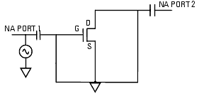
This procedure measures the device S-parameters across the frequency range of operation, with the device in an unbiased condition (that is, with both the gate and drain bias set to zero). Under these conditions, the transconductance and drain conductance are negligible, so the equivalent circuit consists only of the parasitic elements and capacitances. The program calculates the intrinsic parasitic resistance from the measured data.
Device Configuration: The input values you set in this procedure configure the device as shown in the following figure.
Figure 84 MOSFET Bias Configuration for parasitics Measurement
|
|
|
Note
|
|
|
|
|
Make sure you have calibrated the network analyzer before you begin this procedure. Refer to the instructions earlier in this chapter.
|
|
Defining the Instrument States
Perform the same procedure you did for the s_vgvdf measurement. Pay particular attention to the notes listed in that procedure. The instrument states need to be set independently for each setup.
Then return to this chapter and continue.
Setting the parasitics Inputs
Most of the input values for this measurement are factory preset and should not be changed.
| 1 |
Select the parasitics setup. |
| 2 |
Set the current Compliance for vg and vd to any reasonable values: in this unbiased condition, current values to the device will be negligible. |
| 3 |
The Sweep Type is set to CONstant for both vg and vd. |
| 4 |
The vg Value is set to 0 to ground the gate. |
| 5 |
The vd Value is set to 0 to ground the drain. |
| 6 |
The freq inputs set the network analyzer for a linear sweep of the calibrated frequency range. Set the freq Start, Stop, and # of Points to correspond with your broadband calibration. |
Measuring, Plotting, and Extracting
| 1 |
Select Plots > r_f > Display Plot. |
| 2 |
Select Measure/Simulate > Measure. |
| 3 |
When the measurement is complete, select Extract/Optimize > z > Execute. The transform calculates the parasitic R values vs frequency from the measured data and enters them in a file named Para.data. |
| 4 |
The r_f plot illustrated shows parasitic resistance with frequency. The resistance data displayed is the real part of the measured device impedance z.m. |
Figure 85 Example parasitics r_f Data
|
|
| 5 |
If you wish, you can recompute the resistance values over the linear portion of the data only, using the X-low/X-high function as follows: |
| |
• |
Select Setup Variables. A variable table will appear, listing X_LOW and X_HIGH with their default values of 0 or current values. |
| |
• |
Choose a relatively linear portion of the plotted traces. Click at the lower and upper boundary points of the linear portion to make a box on the trace, as shown next. |
Figure 86 Choosing a Relatively Linear Portion of the Traces
|
|
| |
• |
From the plot menu select Options > Copy to Variables. This changes the X_LOW and X_HIGH values in the table to the boundary points you selected. |
| 6 |
Select Extract/Optimize > compute_r > Execute. The transform recalculates the parasitic resistance values as the average of the linear data you defined, and modifies the Para.data file accordingly. The values for rs, rd, and rg are listed in the IC-CAP Status window. |
| 7 |
The parasitic values can be modified after the main data acquisition, just before the model generation. |
Setting Up the Main Data Acquisition
This sets up the values for the main measurement procedure, which takes the data from which the model will be generated. The procedure measures S-parameters at a calibrated CW frequency, across a range of drain and gate bias voltages. It takes adaptive measurements, densely spaced in the most nonlinear regions such as at the knees of the I-V curves and at the onset of breakdown, and less densely spaced in the linear saturation region. The number of data points measured depends on the nonlinear behavior of the device and on the measurement conditions you set up.
Some knowledge of the device characteristics is needed in order to enter valid parameters. The data you measured in the DC and S-parameter preverifications may be useful in determining appropriate values for your device. Do not exceed maximum allowable values. Perform the steps in the following paragraphs.
The data acquisition rate is approximately 700 points per hour. Once you have initiated the transform, the data acquisition takes approximately 1 to 2 hours before your interaction is needed again.
Defining the Instrument States
The instrument states for the main data acquisition are set in the dc_bias and ac_bias setups.
|
Caution
|
|
|
|
|
Do not change the Inputs in the dc_bias or ac_bias setups. Their function is not the same as in the other setups. They contain factory-set information essential to the program, and they must not be changed.
|
|
| 1 |
Select the dc_bias setup. |
| 2 |
Select the Instrument Options tab to display the DC source/monitor instrument states. |
| 3 |
Set the Agilent 4142 instrument state the same as for the idvd_vg DC preverification measurement. |
| 4 |
Select the ac_bias setup, then Instrument Options. |
| 5 |
Note that the instrument states are different for CW and list frequency measurements. Set the instrument states almost the same as you did for the s_vgvdf preverification measurement, with the following exceptions (because you are now using the CW calibration instead of the broadband frequency list cal): |
| |
• |
Set Use User Sweep to Yes. |
| |
• |
Set Cal Set No to the cal set or register where you stored your CW calibration. |
|
Note
|
|
|
|
|
If you fail to use the CW calibration and use the broadband cal instead, the measurement will take a great deal more time than expected. It will measure data at all the bias points at every frequency point. The plotted results will be hard to interpret!
|
|
Setting the Variables
You set the values that define the main measurement and the model generation in the data_acquisition and model_generator transforms in the create_mdl setup. Based on your information, IC-CAP characterizes the device within a subset range of the bias plane (Vd-Vg plane). This range is typically larger than the normal safe range for long-term DC device operation specified in the data sheet. In other words, the device is briefly pushed beyond its long-term normal DC operating range. This is required by the model for simulating large-signal AC and transient pulsed operation, where the instantaneous voltages can temporarily exceed the boundaries of long-term safe DC operation.
| 1 |
Select the create_mdl setup. |
| 2 |
Select the Extract/Optimize tab, and the create_mdl transforms are listed. |
| 3 |
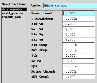
Select data_acquisition to display the variables used in the data acquisition. |
Figure 87 Variables in the data_acquisition Transform
|
|
| 4 |
Follow the steps below to enter variable values appropriate for your device. |
| 5 |
Do not change the Function name at the top of the table. |
| 6 |
For Power level, enter the total maximum power dissipation value. This should typically be 2 watts per mm of gate width for devices up to 1 mm. |
| 7 |
For I Breakdown, enter the reverse gate current breakdown value. |
- The next four voltage values define hard limits to the measurement domain. The voltage values are set well beyond the normal device operating range to explore the device's boundary response. If the values are set too conservatively, data will not be measured in the nonlinear areas of breakdown and maximum forward conduction. If this occurs in the measurement, return to this transform and change the voltage values. Reduce the minimum values and increase the maximum values.
| |
• |
Min Vd should typically be slightly negative, to allow data to be taken slightly beyond the bounds of the model so that it is possible to properly extrapolate beyond the data. |
| |
• |
Max Vd should typically be slightly higher than any anticipated breakdown voltage. |
| |
• |
Min Vg should typically be one to several volts lower than Vthreshold for an NMOS device. |
| |
• |
Max Vg should typically be around the maximum gate operating voltage. |
| 8 |
For Min Step, enter a value to define the step size between densely-spaced measurements. |
| 9 |
For Max Step, enter a value to define the measurement step size where you expect the data to be relatively linear and you do not need densely-spaced measurements. |
| 10 |
For Vth, enter the gate threshold voltage Vthreshold. |
| 11 |
Delta defines a voltage range below Vth where a high density of Vgs measurements is needed due to the nonlinear decrease in drain current at threshold. |
| 12 |
Eps (Epsilon) is used to predict the next point to be measured, and thus control automatic data acquisition step size. Increasing the value of epsilon decreases the sensitivity of the automatic data acquisition. |
| 13 |
For Noise thresh, enter a current threshold value for both drain current and gate current below which you do not need closely-spaced measurements. The automatic step-size algorithm is not used below the Noise thresh value, where measured currents are sampled at the maximum step size. |
| 14 |
For SMU Compl, enter the drain SMU maximum current compliance value in amps. This is the maximum output current capability of the Agilent 4142 plug-in source/monitor unit (SMU) supplying the drain terminal. In the example procedure, this is VD or HPSMU3. For the Agilent 41420A high-power SMU, the compliance is 1A; for the Agilent 41421B medium-power SMU, the compliance is 100 mA. |
|
Caution
|
|
|
|
|
Also be aware of the current ratings of your bias networks, and do not set current values beyond their specified maximum limits. It is quite possible to destroy the bias networks, and the probes, by applying current values beyond the specified limits. (The standard bias networks for the Agilent 85122A/85123A parameter extraction test systems are rated at 0.5 amp.)
|
|
| 15 |
You can save the values in the transform to use for another extraction. Select File > Save As, then the File Type Transform, type an appropriate filename, and select OK. The file is saved with the suffix .xfm. |
Performing the Data Acquisition Measurement
This procedure performs the measurement you defined. Once you initiate the transform, the data acquisition takes approximately 1 to 2 hours to run before your interaction is needed again. The data acquisition rate is approximately 700 points per hour. The number of data points measured depends on the nonlinear behavior of the device and on the measurement conditions you set up.
| 1 |
In the create_mdl setup select the Extract/Optimize tab. |
| 2 |
Select data_acquisition > Execute. During the data acquisition process, a running message in the UNIX window indicates the approximate percentage of completion. |
|
Caution
|
|
|
|
|
Do not perform data acquisition more than once. This will write over the existing data, and will use more time and memory.
|
|
| 3 |
If you do attempt to perform data acquisition after the measurement has already been done, a dialog box will alert you that a measurement file exists. You then have several choices: If you do not need the data in the current file you can select OK or Return to overwrite it. Or you can abort your new measurement by selecting Cancel. Or if you wish to save the measured data and perform another data acquisition, go to a UNIX window, change directories if necessary, find the file Measured.data, and rename it with another appropriate name, then continue with the data acquisition. |
| 4 |
Ignore this message if it occurs: CAUTION: CALSET X STATE MAY BE INVALID. |
| 5 |
When the process is complete, a message similar to the following is shown in the UNIX window: |
- INITIAL Extraction Results
Max_num = 66.00
Max_row = 49.00
Done!
- The numbers are part of the internal function of the program, and irrelevant in user interaction with the program. They are associated with the maximum number of points for a given Vgs, and the number of Vgs steps.
Plotting the Measured Data
The plots in the create_mdl setup provide graphical outputs of the data acquisition and model generation. Most of the plots are of data measured in the main data acquisition. However, Qg and Qd are outputs of the model generator, and will be viewed later.
For hardcopy output, black and white can be reversed for faster printing and easier reading on paper, as explained in the procedure.
If you wish to plot data from a previously stored data set, you will need to perform the steps explained under "To Plot an Earlier Data Acquisition" on the next page. Otherwise, follow these steps:
| 1 |
From the Plots tab, select the plot of your choice, and Display Plot. |
| 2 |
You can augment the annotation of a plot by specifying header and footer labels you wish to print with the data. However, it is essential not to change the Y data input fields. |
| 3 |
To change a plot's annotation, go to the Header or Footer lines in the plot definition. You can type a label of your choice in the header or footer input field (right side of the definition table). Then select Options > Update Annotation, and your label is added to the plot. |
|
Note
|
|
|
|
|
Changing the Y Data input fields can cause anomalies in the measurement and modeling results.
|
|
| 4 |
If you wish to exchange the black and white in a plot for better hardcopy quality, select Options from the plot menu, and Exchange Black-White from the pull-down menu. You can also change from colored traces to all black by selecting Options > Color. This is particularly useful if one of the traces is a light color such as yellow, which may not show well against a white background. |
| 5 |
To get a hardcopy of a plot, from the plot menu select File > Print Setup. Enter the name of a printer and make any other changes to the printer/plotter setup you wish, then select OK. |
| 6 |
If you have your printer setup completed, select File > Print. |
To Plot an Earlier Data Acquisition
If you wish to view data from a previously stored Agilent RootMOS data acquisition, you will need to perform these extra steps to bring the data into this model and display the plots.
| 1 |
From the IC-CAP main menu select File > Change Directory. Type in the path name of the file where your data is stored, and select OK. |
| 2 |
Select the create_mdl setup. |
| 3 |
From the Plots tab, select the plot of your choice, and Display Plot. (The displayed plot window will be blank and an error message will be displayed. Ignore the error message and click OK.) Now select Display Plot again, and the plotted data will be properly displayed. (The first time you selected Display Plot, an internal function re-initialized the data from the changed directory.) |
The Measured Data Plots
The plots listed next illustrate the data measured by the data_acquisition transform for an example device.
| • |
Id_vd plots the DC measurement of drain current Id as a function of Vds for different values of Vgs. Check this plot to see if you are satisfied with the bias range of the measurement. If not, go back to Setting the Variables and make appropriate changes in the values of Min Vd, Max Vd, Min Vg, and Max Vg. |
| • |
Y11i plots the imaginary part of the Y11 admittance data. |
| • |
Y12i plots the imaginary part of the Y12 admittance data. |
| • |
Y21r plots the real part of the Y21 admittance data. |
| • |
Y22r plots the real part of the Y22 admittance data. |
| • |
Vd_Vg plots the distribution of test data in the Vgs-Vds plane. It shows how the data is taken adaptively depending on the device nonlinearities. More test data is taken where the device characteristics change rapidly such as at the knees of the I-V curves and the onset of breakdown, and less in the linear saturation region. |
If you are satisfied with the measured data for your device, proceed to the model generation. Be sure the limits of the measurement domain are adequate: the domain should extend beyond the normal operating range of the device. If the measured data does not show the limits of device behavior, you may wish to redefine the voltage ranges you set in the data_acquisition transform, using values that are less conservative, and perform the data_acquisition again.
Generating the Model
This procedure calculates the model parameters from the measured data, and generates a corresponding model for the device. The model nonlinear functions are calculated by contour integration, therefore you must provide the program with a starting point for the contour integration.
If you are generating a model from a previously stored data set, perform the steps listed later in this procedure under Generating a Model from Previously Measured Data.
Computing the Parasitics for the Model Generation
An earlier part of the procedure calculated the intrinsic parasitic resistances of the device and entered them in the file Para.data. Now this procedure updates the data and gives you the opportunity to override the calculated values and input values of your own if you believe they are more appropriate.
Select the main DUT, and the DUT Variables tab. A variable table is displayed, showing current values for the intrinsic parasitic resistances and inductances, as well as other variable values. The following figure illustrates the DUT variables table. Note the intrinsic inductances Ls_tot, Ld_tot, and Lg_tot all have default values of 1.000f.
Figure 88 Variable Table of the main DUT, Showing Parasitic Values
|
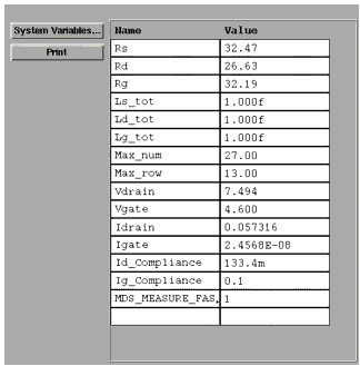
|
Do not change any of the other variable values in the table besides the R and L values. The other variables listed are internal functions necessary to the program, and can be ignored.
If you have reason to change any of the parasitic values, you can change them in this variable table. For example, if you have calculated the parasitic values by another method, such as from material measurements or by using a different algorithm, you may prefer to use those values. Or based on the model generation results plotted later in the procedure, you may wish to return to this step and modify values, then perform the transforms again.
|
Note
|
|
|
|
|
If you make any changes to the parasitic values in the variable table, do not perform the compute_para transform.
|
|
If you do not wish to make changes to the parasitic values, select the compute_para transform in the create_mdl setup, and Execute. You will probably observe changes in the parasitic values in the table.
|
Note
|
|
|
|
|
You can copy the variable table by selecting Detach to display it in a separate window. Resize the window and move it to a convenient place away from the central work area.
|
|
Setting the Starting Point for Contour Integration
|
Note
|
|
|
|
|
For the modeled nonlinear functions to be valid, contour integration must be done in the normal operating range of the device. Outside the range, the results will be very different and less accurate. The further from the operating range, the less accurate the model will be.
|
|
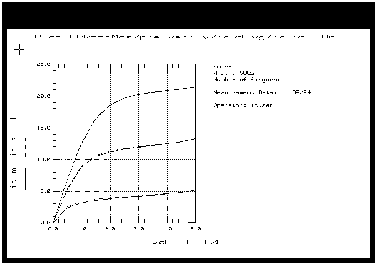
Use the following guidelines to set the starting point of contour integration:
| 1 |
The starting point should be set at an intersect of Vd and Vg that is within the saturated class A operating range of the device, where drain voltage is beyond the knee and less than breakdown, and gate voltage is between Vthreshold and Max Vg. |
Figure 89 Example of Appropriate Contour Integration Starting Point
|
|
| 2 |
If you know Vthreshold and Vbreakdown, set: |
| |
• |
Vthreshold < vg_start < vgmax*, and
Vknee < vd_start < Vbreakdown |
- or
| |
• |
vg_start = Vthreshold/2, and vd_start = Vbreakdown/2 |
- (*vgmax is the approximate gate voltage corresponding to the maximum device drain current for a typical drain voltage in saturation. vgmax is generally lower in magnitude than Max Vg.)
- Figure 89 shows an appropriate value for the contour integration point of an example device, marked with a + on the plot.
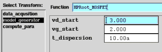
Setting the model_generator Variables
| 1 |
Select create_mdl > Extract/Optimize > model_generator. The table illustrated below is displayed. |
Figure 90 Variables in the model_generator Transform
|
|
| 2 |
Enter an appropriate value for vd_start. Note that for a PMOS device this will be  0V. 0V. |
| 3 |
Enter an appropriate value for vg_start. Note that for a PMOS device this will be 0V. |
| 4 |
Enter an appropriate value for t_dispersion. This is the dispersion time constant, and its default value is 1e-17 or 10 attoseconds, 10.00a. In most cases, t_dispersion is not a significant factor although it is used in the model generation calculations. However, in a case where you wish to add time dispersion effects, you can increase the value. |
Executing the Model Generator Transform
| 1 |
Select Execute to start the model_generator transform. |
| 2 |
A dialog box asks you for an MDS file name. The standard file generated by the model for interface with MDS is named State.mds. If you want to retain this filename select OK or press Enter. Otherwise change the name to a new filename that associates this model with the device, retaining the suffix .mds for compatibility with MDS. |
|
Note
|
|
|
|
|
If you plan to do a verification, retain the filename State.mds for now, as the verification process requires this filename. You will have another opportunity to change the filename after the verification process.
|
|
| 3 |
The model generation takes a few seconds. A Done! message in the UNIX window indicates the model generation is complete. |
Generating a Model from Previously Measured Data
If you wish to generate a model from a previously stored measurement, you will need to perform these additional steps to bring the data into this model in the correct form.
| 1 |
From the IC-CAP Main window select File > Change Directory. Type in the path name of the file where your data is stored, and select OK. |
| 2 |
Select the create_mdl setup. |
| 3 |
Select compute_para > Execute. |
Plotting the Generated Data
In the create_mdl setup, the Qg and Qd plots show the calculated state function data generated by the model_generator transform.
|
Note
|
|
|
|
|
The modeled state function data will not be plotted unless the init_parameters macro has been executed (see the instructions near the beginning of this chapter). The icplotnotes file generated by the init_parameters macro provides the x-axis information needed to plot the modeled data. IC-CAP will display an error message if you have not executed the init_parameters macro.
|
|
| 1 |
From the Plots tab, select the plot of your choice, and Display Plot. |
| |
• |
Qg is the distribution of charge current under the gate. The illustration shows this data for an example device. |
| |
• |
Qd is the distribution of charge current under the drain. |
Other Outputs of the Model Generation Process
The model generation process results in a number of different output files to be used for different purposes. These include the model file for MDS interface, data on various modeled parameters, measured device data, and files for internal use by the program.
Some files have default filenames assigned by the program. Others may be files you created during the procedure to save device-specific information.
|
Caution
|
|
|
|
|
In general, the files should NOT be modified, because changing them can cause problems that may invalidate the model. It is also important that you do not change the names of files created by the model generator, with the exception of State.mds.
|
|
Following is a list of some files that will be or may be created during the modeling process:
| • |
icplotnotes. This is the only file you can safely edit or add to. The program appends it as a label to any graphical outputs, to identify the device. It includes a device ID string and any additional information you choose to add to graphs when they are plotted. |
| • |
icplotnumbers. This is an internal file used by the program to generate a graphical interface. It is related to the Max_num and Max_row messages that appear in the variable table of the main DUT and in the UNIX window at the end of the data acquisition. While these parameters are irrelevant to user interaction with the program, they are essential to its function, and they must appear on-screen. Do not change this file. |
| • |
Measured.data. This is the raw measured S-parameter data as a function of bias and frequency, produced by the create_mdl data acquisition process. |
| • |
Para.data. This is the S-parameter vs frequency data with the device in an unbiased condition, used by the program to calculate parasitic resistance and inductance values. |
| • |
State.data. This file is used by the program in plotting nonlinear functions such as Qg and Qd. Do not change this file. |
| • |
State.mds. This is the model file used by the Agilent RF and Microwave Design System (MDS) in a circuit simulation. It is also used in verifying the model, and needs to retain the name State.mds in the verification process in order to maintain the MNS simulator link. However, since every Agilent RootMOS model initially has this name, you change the name to identify the device, either when you execute the transform to generate the model (if you are not performing a verification), or at a later time as described at the end of this chapter. |
| • |
Y.data. This file contains the Y-parameters as a function of bias, to examine through graphical interface. NO changes can be made to the Y.data file, except for adding header and footer labels as explained under Plotting the Measured Data. |
| • |
dc_test.set (or some other name designated by you). If you decided to save it, this is the measured DC data generated in the idvd_vg DC preverification procedure. |
| • |
spar_test.set (or some other name designated by you). If you decided to save it, this is the measured S-parameter data generated in the s_vgvdf S-parameter (AC) preverification. |
Verifying the Model DC Data
This procedure verifies the model DC data against the DC data measured in the idvd_vg preverification setup, using the MNS simulator link.
|
Note
|
|
|
|
|
The simulator used must be MNS. If the SIMULATOR in the model variable table is set to another value, change it to mns.
The name of the model file must be State.mds for the purposes of verification, to maintain the MNS simulator link.
|
|
| 1 |
Select the idvd_vg setup. Make sure the output Type is set to B for both measured and simulated data. |
| 2 |
From the Plots tab, select the id_vd plot, and Display Plot. |
| 3 |
Select Measure/Simulate > Simulate. |
Figure 91 Example Measured and Simulated id_vd Data
|
|
| 4 |
Check that the simulated data (dotted line) and measured data agree. The illustration shows example measured and simulated id_vd data. |
Verifying the Model S-Parameter Data
This procedure verifies the model S-parameter data against the S-parameter data measured in the s_vgvdf setup, using the MNS simulator link.
|
Note
|
|
|
|
|
The simulator used must be MNS. If the SIMULATOR in the model variable table is set to another value, change it to mns.
The name of the model file must be State.mds for the purposes of verification, to maintain the MNS simulator link.
|
|
| 1 |
Select the s_vgvdf setup. Make sure the s output Type is set to B. |
| 2 |
Select Plots > Display All. Two S-parameter plots are displayed. |
| |
• |
s11_s22 shows example measured and simulated S11 and S22 data |
| |
• |
s12_s21 shows example measured and simulated S12 and S21 data |
| 3 |
Select Measure/Simulate > Simulate. Check the agreement between the simulated data (dotted lines) and measured data. |
Storing Your Model and Interfacing with MDS
Once you have developed your device model, you can store it in a file for future use. You can use it for circuit simulation in the Agilent RF and Microwave Design System, inserting it into circuits under design to emulate the characteristics of your device. It can be used to represent any device with the same geometry from the same process, or scaled to represent a different-sized device. It will predict the gain, power, gain compression, and harmonics performance of the device as a component in circuits you design using MDS. It will predict large-signal device operation over a range of bias points and loading conditions.
The file generated by the modeling process for interface with MDS is called State.mds. You need to change the name to one that will identify the device under test, since every Agilent RootMOS model file is initially named State.mds.
If you chose not to perform a verification, you may already have changed the filename using the dialog box presented before the model_generator transform. If not, you can change the filename now in UNIX and store the file as follows:
Storing the Model
| 1 |
Use the UNIX directory you created at the beginning of the procedure, when you first opened the model file. |
| 2 |
From the IC-CAP Main window select File > Save As. |
| 3 |
A dialog box is displayed. Select the desired File Type (for example, .mdl for a complete model). |
| 4 |
Select a new filename that associates this model with the device. |
| 5 |
Use the UNIX cp command to copy the file State.mds to the new filename, including the path name of the designated directory. Select OK. |
This completes the example Agilent Root MOSFET measurement and model generation procedure. For an explanation of how to use IC-CAP model data in MDS, refer to Appendix D, "Using IC-CAP Data with MDS."
|