Print version of this Book (PDF file)
DC and CV Measurement of MOSFET's for the MOS Models
This section provides information to make the necessary measurements of your devices. It will provide information on features of the MOS Modeling Packages and how to use the graphic user interface (GUI). For hints on how to measure and what to measure using the right devices, see Chapter 3, "PSP Characterization, Chapter 4, "BSIM4 Characterization", and Chapter 5, "BSIM3v3 Characterization".
Since the measurement module of the MOS Modeling Packages are identical, we describe only one of them in detail.
Note
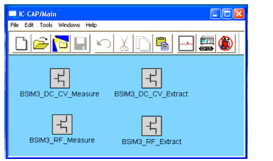
The GUI is opened by double clicking the BSIM3, BSIM4, or PSP Icon which appears in the IC-CAP/Main window after you open one of the example files. To open an example file, click File > Examples > model_files > mosfet > bsim3 (or bsim4 or PSP) then select a Measure or Extract model file. Figure 1 shows four of the files in one IC-CAP/Main window, using BSIM3 as an example.
Figure 1 Starting the BSIM3 GUI from IC-CAP/Main window
After you have double clicked the icon, the GUI window of the MOS Modeling Packages (Figure 2) appears on your screen.
Figure 2 Part of the Graphic User Interface for the MOS Modeling Packages
The top row of the GUI shows the File, Configuration, Data, Tools, and Help menus. Some menu topics are only activated when using specific tasks (depending on which folder is activated!). For example, if you are setting up the conditions for a Temperature measurement, the Configuration menu only allows you to add or delete temperatures. The rest of the menu is not active since it is not necessary to set or sort categories during temperature setup, for example.
The File menu has entries to Import and Export list and measurement data from measurement software other than IC-CAP. Those functions are described in Import Wizard.
The standard IC-CAP icons (from left to right) are located below the menu. Use these icons to create a New, to Open an existing, to Copy and Open an Example, to Save Setups or Entries, to Measure, to Display and Close plots, to Add or Delete, to define Temperature Measurements, to Set categories, or to Check SMU connections. You will be prompted before the selected action takes place. Again, some of the icons are only activated when specific folders are active.
The lower part of the window displays the project name and project directory.
To Print a setup, choose File > Print Setup. This opens a dialog box. In this dialog box, enter the command line for your specific printing device and choose OK. The folder will be printed.
On Windows operating system, the command line is print /d:<printer name>. For example, if the printer is connected to a server named MYFS1 and the printer is named MY0017, type:
Note
If you don't enter a printer command, the output will be redirected to the IC-CAP/Status window.
Note
From the Help menu you can choose between browsing the Topics or getting help for each of the different task folders described below. There are in depth hints for the task, for example, which device geometries to use or how to connect the instrument to the device under test to get the best extraction results from your measurements. You will find links that bring you to Chapter 3, "PSP Characterization", Chapter 4, "BSIM4 Characterization", or Chapter 5, "BSIM3v3 Characterization". Use your Browsers Back button to return to the location you were at before following the link.
Below the top row of icons are five folders. Basically, each folder is assigned to a specific task in the measurement process. They are intended to be parsed from left to right, but you are not bound to that order. Some entries into one or the other folder will change settings on another folder.
For the new user: You should process the folders in the order from left to right.
Each of the following sections describe one folder of the GUI. BSIM3, BSIM4, and PSP model folders are usually equal to each other.
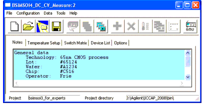
Project Notes
The notes folder is provided to store notes you take on a specific project. You can enter general data like technology used to produce this wafer as well as lot, wafer, and chip number. There is a field to enter the operator's name and the date the measurement was taken. Space has been provided to enter notes on that project.
Notes entered into the measurement module will be transferred to the Information folder inside the DC_CV_Extraction modules.
Temperature Setup
Use this folder to define measurements at specified temperatures. Basically, the measurement of all DUTs is performed at SPICE default temperature TNOM, which is set to 27° Celsius.
To change the default value of 27°C to represent your measurement temperature, double click and enter the actual environment temperature inside your measurement lab into the TNOM field.
Note
Add new measurement temperatures using the Add icon or the Configuration menu. If you no longer need a measurement temperature, click the Delete button. You will be prompted for the temperature to be deleted. If there is a file containing measured data for this temperature, the data file will be deleted if you choose OK on the prompt dialog.
The delete window does not contain an entry for the temperature set as TNOM, since TNOM cannot be excluded from measurement and extraction.
Don't forget to enter the actual temperature in degree Celsius (°C) into the TNOM field during measurement of the devices.
Note
When you add a new measurement temperature, a new column is added to the Device List folder's Device List table for DC Transistor, Capacitance, and DC Diode.
Any changes on the Temperature Setup folder must be saved prior to selecting another folder.
Switch Matrix
Use this folder to define which measurements use a switch matrix (see Figure 3). There are three options: Use a switch matrix for DC Transistor Measurements, for Capacitance Measurements, and for Diode Measurements. You can select any one or more than one by checking the appropriate boxes.
Assignments must use SMU1....SM4. This assignment is done inside the hardware setup of IC-CAP. Usually, the default of the appropriate DC-CV-Analyzer is SMU1...4. In rare cases, such as the Agilent E5250 for example, the default SMU number corresponds to the slot number of the module inserted into the instrument. If your E5250 uses 4 SMU's at slot No. 1, 3, 5, 6, the default names of the SMU's are SMU1, SMU3, SMU5 and SMU6. You must change this default names to reflect SMU1, SMU2, SMU3 and SMU4 to properly communicate with the BSIM3/4 and PSP modules.
Note
To change or enter the names of the Source-Measurement-Units (SMU's), open the model for editing then go to the folder DUTs/Setup, subfolder Measure/Simulate. Configure the different inputs/outputs there.
Note
Figure 3 Defining the use of a switch matrix for measurements
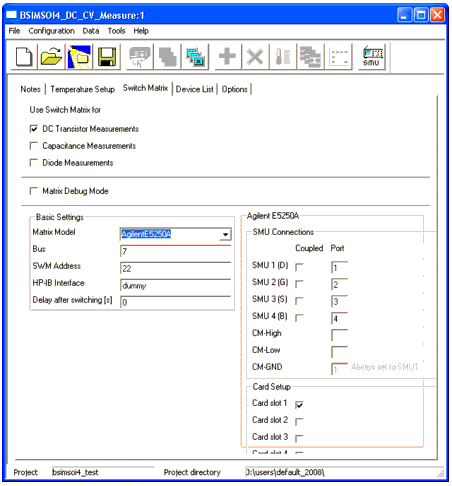
The Basic Settings provide a choice of several different Matrix Models, which are supported by IC-CAP. Type the appropriate Bus and GPIB address of the Switch Matrix (SWM Address; 22 in our example) as well as the GPIB-Interface name. See the IC-CAP Reference manual for a complete description of the GPIB settings for the selected switch matrix. Our example shows the use of an Agilent E5250A matrix model. For this type of instrument, you have to define which port is connected to which SMU or C meter input pin and which slot is equipped with a card.
Again, you have to save your changes prior to leaving this folder.
The actual pin connections are entered into the DUT Variables folder for the measurement selected to use a switch matrix (one or more of the DC Transistor, Capacitance, or Diode Measurements). For example, if you've selected DC Transistor Measurements to use with a switch matrix, you must open the model file for editing and in the DUT/Setups folder select the DC Transistor then in the DUT Variables folder enter the switch matrix pin numbers in the fields below the node names. This is especially useful if you would like to make series measurements on wafers using a probe card (e.g., for quality control).
For automatic measurements, macros are available. These macros enable you to make automatic series measurements of complete dies or arrays. They are created for automatic measurements with or without heated chucks.
For example, open the IC-CAP model for BSIM3_DC_CV_Measure (from the IC-CAP/Main window, right click the DC_CV_Measure model then select Edit). The Macros folder contains a macro called Example_Wafer_ Prober.
You will also find a macro in the $ICCAP_ROOT/examples/model_files/mosfet/BSIM3/ examples/waferprober directory named prober_control.mdl. Please use this macro or model file and tailor it to your needs. There are readme sections to explain the steps to be taken inside the macros.
The automatic measurement of model diagrams using the macro works without involving the GUI.
For your convenience, the waferscan macro in the prober_control.mdl example model file can be loaded into IC-CAP and can be run in a demo mode without taking actual measurements.
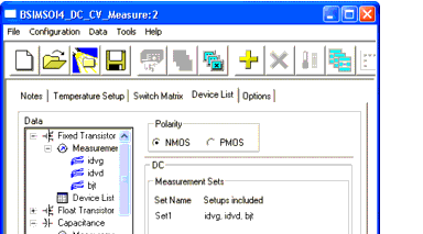
Device List
The next step in the modeling process is setting up measurement conditions for different measurement tasks like DC, Capacitance, or Diode measurements and to enter the devices to be used.
This folder is designed for easy setup of conditions for DC Transistor and Capacitance as well as DC Diode measurements. Figure 4 shows the folder used for setting up measurement conditions as well as the devices to be measured. Use the Icons or the menu to save this folder prior to proceeding to the next task.
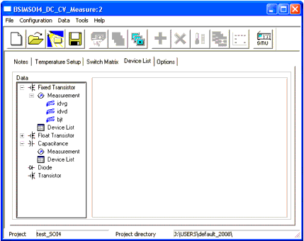
The left side of this folder shows a tree view of the data for this measurement project. This tree definition may be different for different models. The previous figure shows the tree used for extracting SOI device parameters.
The folder shows entries not normally present on BISM3/4 or PSP measurement projects. For example, there are no floating transistors to be measured in BSIM3 or 4 modeling tasks.
To expand the Transistor, Diode, and Capacitance entries, click the + sign to reveal a Measurement and Device List.

By clicking on Measurement, the right side of the folder shows predefined measurement sets as well as setups already selected for the specific measurement. To add a setup, click the ![]() icon.
icon.
You will be prompted to select a setup and enter a name for it. The new setup will be included in the tree below Measurement.
If you select one of the measurement setups inside the tree, the folder changes to reflect the measurement conditions valid for the selected setup.
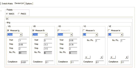
Figure 5 Measurement Conditions for the idvg-setup
On that form, you can enter the polarity of the devices to be measured and define the conditions for DC measurements as well as to specify current limits for the SMUs (compliance settings).
Polarity
There are polarity buttons to specify whether you are measuring NMOS or PMOS devices. Select NMOS or PMOS. Our example shows the measurement of NMOS devices.
Compliance
DC Compliance settings for the source measurement units (SMUs) are located at the bottom row of the form. You can set different compliance values for each SMU.
DC
The Measurement Data tree uses setups to define different measurement configurations. For compatibility reasons with former versions of IC-CAP, there are two basic setups provided: One called idvg for measuring the drain current dependency from the gate voltage of the device (e.g., transconductance of the device). The other one called idvd for measuring the drain current dependency from the drain voltage, the so called output characteristics of the device.
| • | idvg: Transconductance (ID=f(VG)) |
This part of the measurement conditions is designed for transfer diagram measurements. Again, there is a choice between a Linear sweep and a List of discrete voltage values, where you can enter a number of points and their respective value. For Linear sweep mode, you specify Start, Step, and Stop voltages for gate, bulk, and drain nodes. Stop value of drain voltage is set to a fixed value in order to measure the relevant range of voltages for proper extraction of the parameters used to model this device behavior.
If you set a Constant value for one of the sources, internally a list with just one entry is being used.
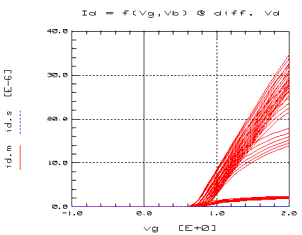
Figure 6 shows the typical form of a transconductance diagram.
Figure 6 Transconductance diagram
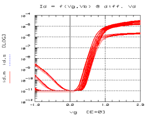
If you change the settings of the diagram in the figure above, one of the effects appearing in submicron semiconductor devices becomes visible. The following figure shows a typical transconductance diagram using a logarithmic y-axis to show the influence of the GIDL (gate induced drain leakage) effect on transistor behavior.
Figure 7 Transconductance diagram showing GIDL effect
| • | idvd: Output characteristics (ID=f(VD)) |
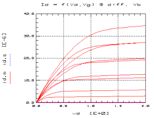
Here you specify the stimulus voltages used for measuring the output characteristic of your devices. You can choose either a Linear sweep or a List of discrete voltage values where you enter a number of points and their respective value. For Linear sweep mode, you define Start, Step, and Stop voltages for drain, gate, and bulk nodes, respectively. Figure 8 shows the typical measured output characteristic of a MOSFET.
Figure 8 Output diagram of a MOSFET
The setups previously described cover the required standard measurement procedure and represent the minimal configuration necessary. The purpose of sweep type LIN(Vt) is to reduce measurement time by excluding areas of the output diagram that are not relevant for extraction. The following figures should help clarify this case.
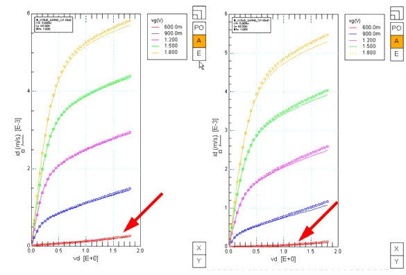
Figure 9 Output characteristic of the same device measured at different values of bulk voltage: left: vb = 0, right: vb = -1.2V
The gate voltage vg in the diagrams shown above has a fixed sweep from 0.6 to 1.8V. Because the bulk voltage changed, the threshold voltage changes, which in turn changes the output characteristic too. The curves marked with a red arrow are measurements at low current levels and therefore need a considerable amount of time due to the integration of noisy currents. Therefore, the lowest gate voltage consumes a lot of time with minimal benefit for the extraction. For example, it would be better to start the left hand diagram at vg = 0.7V and the right hand diagram at vg = 0.8V. This can be achieved by making the gate voltage sweep starting points dependent on Vth of this device.
The LIN f(Vth)-sweep is a linear sweep using a starting value dependent on an extracted threshold voltage value from another Vg-type sweep.
This sweep needs a reference to another sweep of type vg. The stop condition is fixed and the start point is depending on the threshold voltage of the reference sweep. If this sweep is selected, the setup must not have any other sweeps (e.g., vb, vs, ...) because the IC-CAP rectangular data format does not support it. The referenced sweep must include the vb, vs, (ve) value of the actual sweep, which is defined to be a constant value. In the case of vd (1st sweep), the threshold voltages in the reference sweep at all vd values are taken and a mean value is generated.
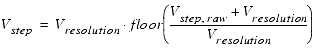
Furthermore, it is necessary to specify a resolution value in order to send reasonable voltage values to a measuring instrument. Taking this into account, the effective start and step values are calculated according to the following formulas:
The following table shows the minimum source configuration. It is now possible to select an output from each source, for example, ig, ib, id, is. The source's output current is in bold letters to indicate that it was used as the minimum required output.
LIST
CON
LIN
LIST
LIST
CON
LIN f(Vth)
LIST
CON
LIN
LIST
When selecting LIN f(Vth), restrictions apply to the sweep options that are underlined in the table above.
To configure a LIN f(Vth)-sweep, select the idvd-setup and choose LINf(Vth) from the Vg pull-down list of sweep types. See the following figure.
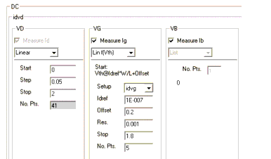
Figure 10 Part of the Device List folder with sweep type Lin f(Vth) selected
Choose an appropriate vg type setup (idvg in our example), and set Idref, offset, resolution (res), stop value, and the number of points (No.Pts.). The vg start voltage value will be calculated using this settings.
If you would like to add measurement setups, choose Configuration > Add from the menu or use the appropriate icon from the top row of icons. A window opens for you to select one of the standard setups and to enter a name for the copy of this setup. By clicking Add, the new setup will appear inside the list of setups. It will use the same settings as defined in the standard setup from which it was created. Adjust all the settings for this new setup according to your needs.
A newly created setup must be configured into a measurement set, which in turn can be used to measure the devices.
Click Configuration > Configure Measurement Setup, or use the configure icon, to open a window for creating a new measurement set or to add a newly created setup to the standard measurement sets. Just click the desired setups to be added or use the Add button to create a new set. Thus, you are able to define measurement sets measuring data from different setups.
Transistor Device List
Select Device List from the tree to enter the devices to be measured. When creating a new project, the device list contains predefined device names that you can simply overwrite with device names of your choice.
The device list table contains additional columns for each temperature you've entered on the Temperature Setup folder.
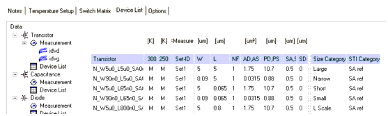
Figure 11 Device List tree with entries for the devices to be measured
The column named Measure shows the allocation of measurement sets to the devices. For each device, you have to select a measurement set to be used for this device. Using the Device List, you can define which set will be used for which device. Select Configuration > Configure Measurement Set to display a list of devices to be measured. Select a device, then select one of the available measurement sets you wish to assign to this device and click OK.
Selecting Configuration > Configure Measurement Set from the menu actually has two different meanings, depending on the subfolder selected from the tree. If the Measurement subfolder is selected, Configure Measurement Set means to add a new measurement set to the list of available sets. If the Device List subfolder is selected, then you can define which set to use for which device.
Note
The Device List under the Transistor branch in the tree view is used to enter DUT names, geometries, and connections to the appropriate DUTs. Since there are differences between the BSIM3 and BSIM4/PSP models, some parameters are to be used only inside the appropriate model and only activated there. The BSIM4/PSP models enables stress effect modeling, which is not possible in BSIM3. Therefore, all stress effect parameters are only used inside the BSIM4/PSP Modeling Packages and are activated only there.
The Configuration menu enables you to set BSIM4/PSP-specific values. You can use different area and perimeter values as well as Number of Squares for the Drain and Source regions of the transistors to be measured (AS, AD, PS, PD, NRD, NRS). Further on you can set stress effect parameters SA, SB, SD. See Stress Effect Modeling for details.
If you deactivate one of the Configuration menu points (AS=AD, PS=PD, for example), additional columns appear in the Device List table.
Now you can enter STI-related parameters. Refer to Figure 15 for details on these parameters.
Well Proximity Effect
Taken from: P. G. Drennan, M. L. Kniffin, D. R. Locascio "Implications of Proximity Effects for Analog Design"; to be found at http://www.ieee-cicc.org/06-8-6.pdf
Highly scaled bulk CMOS technologies make use of high energy implants to form the deep retrograde well profiles needed for latch-up protection and suppression of lateral punch-through. During the implant process, atoms can scatter laterally from the edge of the photoresist mask and become embedded in the silicon surface in the vicinity of the well edge, as illustrated in Figure 12. The result is a well surface concentration that changes with lateral distance from the mask edge, over the range of 1um or more. This lateral non-uniformity in well doping causes the MOSFET threshold voltages and other electrical characteristics to vary with the distance of the transistor to the edge of the well. This phenomenon is commonly known as the well proximity effect (WPE).
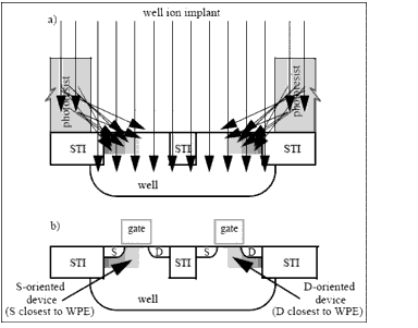
Figure 12 Well Proximity Effect: a) caused by ion scattering during well implantation; b) Orientation of devices inside the well
The Well Proximity model considers the influence of the effect on threshold voltage, mobility as well as body effects.
The Configuration menu contains a selection to activate the well proximity effect, or WPE. Activating the well proximity effect inserts additional rows for WPE parameters SCA, SCB, SCC, and SC into the device list. It is possible to enter SC only after selecting the respective menu item from the Configuration menu. If this option is chosen, parameters SCA, SCB, and SCC are calculated from SC-they cannot be modified once this option is set. They will be updated as soon as you enter an SC value and select save.
SC is defined as "The distance to a single well edge used in calculations of SCA, SCB and SCC when layout information is not available". If SCA, SCB, and SCC are not given due to lack of detailed layout information, their estimation can be made by simulators based on the assumption that for most layouts, the devices are close to only one well edge.
For details, see the BSIM4 manual from the University of Berkeley. Their website contains a link where you can download the complete manual. The address is http://www-device.eecs.berkeley.edu/~bsim3/bsim4_get.html
Defining Devices
For your convenience, there are predefined DUTs on the Device List folder when creating a new project. You can either use those predefined DUTs, only adjusting names, device geometries, connections and so on, or you can delete existing DUTs and add your own.
| • | Choose Add from the row of icons or Configuration > Add from the menu. You will be prompted for the DUTs to copy. Select the desired names and choose Add from the Add DUT window. It is also possible to set the number of copies of the selected DUTs. Added DUTs will automatically get the extension "_new" to the name of the original DUTs. |
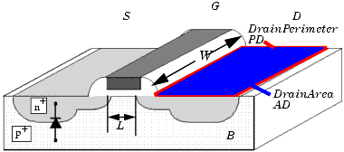
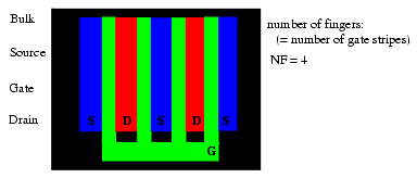
For each line, enter a name for the DUT, gate length and width (L, W), drain and source areas (AD, AS), perimeter length of drain and source (PD, PS), and the number of device fingers (NF) of the transistor to be measured. If modeling stress effects in BSIM4 or PSP, enter SA, SB, and SD as well. See Figure 13 as well as Figure 14 for details on device geometry, respective Figure 15 for details on STI modeling parameters. Well Proximity modeling requires the entry of parameters SCA, SCB, SCC, and/or SC.
Geometries
Shown in the following two figures are views of MOSFET's, where you can find the geometries required by the BSIM3 and BSIM4/PSP Modeling Packages.
Figure 13 .Cross section of a MOSFET showing device geometries
You are not bound to an order of entry. This means, you are not required to begin with the large transistor, the short transistor or the narrow one. Just type in the geometries into each line as you like.
Figure 14 Top view of a multifinger MOSFET
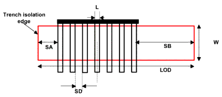
In addition to the standard BSIM4 definitions, columns for SA, SB and SD are available, see Figure 15 for a definition of the parameters used in shallow trench isolation modeling.
Figure 15 Shallow Trench Isolation related parameters
Moreover, each transistor is assigned to two different categories as is described in the following section.
Categories
The Device List shows one or more category columns, depending on what you are extracting: The first one is the size category, the second one is the STI category, and the third one is the WPE category.
| • | Size category (applicable for BSIM3 and BSIM4/PSP): determines the properties of a transistor regarding channel length (L) and width (W). |
| • | STI category (applicable only for BSIM4/PSP): determines the properties of a transistor regarding the actual value of SA/SB. Mainly, this category defines, whether a device belongs to the reference values SAREF, SBREF or has SA, SB values, which are different from the reference values. |
| • | WPE category: determines the properties regarding the well proximity effect. |
Devices at SA=SAREF and SB=SBREF are used to determine all other model parameters except the STI related parameters.
Note
The Configuration menu enables you to Sort the entries into an order or to Set the size category of your devices manually. See Transistors for DC measurements.
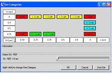
You can use Configuration > Sort or the appropriate icon to set the size category of your devices automatically. Otherwise, you are required to enter the size category manually using the form shown in Figure 16.
The device category is used for extraction purposes. See Transistors for DC measurements in the BSIM3 Characterization chapter for an explanation of categories and requirements for proper extraction of device parameters as well as the paragraph about Stress Effect Modeling inside Chapter 4, "BSIM4 Characterization".
If you would like to delete devices:
| • | Choose Delete from the row of icons or from the Configuration > Delete menu. You will be prompted with a list of DUTs. Select the DUTs to be deleted and choose Delete on the Delete DUT form. A prompt dialog box appears. Select OK if you are satisfied with your choice of DUTs to be deleted. |
According to your choice of temperatures on the Temperature Setup folder, one or more columns marked with the temperatures you have entered appear. The fields of those columns show either (0) for no measured data available, (M) for DUT already measured or (-) for DUT not to be measured at that temperature.
| • | To select devices to be measured at different temperatures: Choose Temperature Measurement from the icons or from the Configuration menu. You will be prompted with a list of DUTs. Select the devices to be measured at those temperatures entered in the Temperature Setup folder and click OK. You can select more than one DUT at a time for temperature measurement by repeated clicks on each one you want to choose. |
You cannot prevent a DUT from being measured at TNOM. All DUTs are measured at that temperature. If you have entered one or more temperatures (T1 and T2, for example) on the Temperature Setup folder, the DUTs selected for temperature measurement are all measured at those temperatures. In other words, you cannot select a DUT for measurement at temperature T1 but not at temperature T2.
Note
To extract temperature effects on parameters, a large, a short, and a small device is necessary!
Note
You can enter a comment for each DUT. If you are using a switch matrix, you can enter a module name and the pin numbers of the switch matrix pin connections to the transistor in the fields below the node names (those fields are present only if the use of a switch matrix is selected on the Switch Matrix folder). See Figure 17 for details.
For the Agilent E5250, the port number to be entered consists of 3 numbers.
If, for example, SMU1 is to be connected to Card No.1, Port No. 3: Enter the number 103 into the field below the transistor's node name. Port No. 12 for Card No. 4 would have to be entered as 412.
Note
When using module names to measure devices with probe cards, pay attention to the node numbers you are entering. Each device uses 4 connections to the switch matrix. You have to enter the correct pin numbers for each DUT and must not exceed the total pin count for each port of your matrix.
Note
Connections to the DUTs
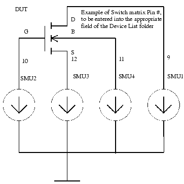
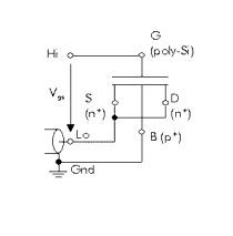
The following figure shows an example for a connected device under test (DUT) to the source measurement units (SMUs) during DC Transistor measurements. The node numbers shown are to be entered into the fields on the Device List folder, see Figure 11. The above mentioned figure shows "0" under all terminal names. Those numbers have to be changed to "10" for the gate, "12" for the source, "11" for the bulk, and "9" for the drain terminal to reflect the connections used inside the following schematic. Please be careful to use the names SMU1...SMU4 during hardware setup in IC-CAP, since these are required by the measurement module of the BSIM3/4 and PSP Modeling Packages.
Figure 17 SMU connections to the device under test
Measurement of the Devices
Once all DUTs are entered with their respective geometries, switch matrix pin connection, and measurement temperatures, the actual measurement of devices can take place. For this purpose, you can use predefined measurement sets if you use the standard measurements called idvg and idvd.
If you've designed a specific measurement for your purposes, you can also define a Measurement Set for those measurements. Select the Measurement subtree and Configuration > Configure Measurement Set from the menu. A window opens where you can define a name for the new measurement set and the measurement, for which this set should be used.
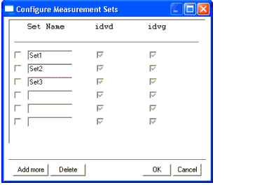
After selecting OK, the newly defined set appears in the list of available measurement sets.
Now you can assign the measurement sets to your devices. For this purpose, select the Device List inside the tree view, then select Configuration > Configure Measurement Set from the menu.
A window opens for you to select the appropriate measurement set to use for each of your devices to be measured.
The following figure shows the Assign Measurement Sets to Devices window. Select a device, then select one of the available Measurement Sets to use for this device. The list - and the appropriate column on the Device List subfolder - will be updated to reflect the actual assignment of Measurement Sets to Devices.
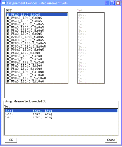
Figure 18 Configuration of Measurement Sets
Starting the measurement of the devices
You will find an appropriate icon inside the row of icons or you can use Data > Measure from the menu.
| • | To start measurement of the devices: Click the Measure icon |
For your convenience, you will find a supplemental model file called "prober_control.mdl" which is suitable to be used with automatic temperature measurements under the directories $ICCAP_ROOT/ examples/modelFiles/mosfet/BSIM3(4)/examples/waferprober. Tailor this model file to your specific Thermochuck model and requirements. Otherwise, be sure to set chuck temperature manually!
Note
If you select measurement of a module, all DUTs in this module are measured automatically if the use of a switch matrix is activated.
The DUTs/Setup folder in the BSIM3/4_DC_CV_Measure model contains an AutoMeasure setup for the Configuration DUT. Using this AutoMeasure setup, you can program automatic measurements for all DUTs in one module.
Automatic measurement uses a macro for the wafer prober. This macro is programmed to start measurement as soon as the wafer prober has reached its programmed destination.
Note
You'll find the macro "Example_Wafer_Prober" and it's transforms together with a description of the transforms in the Macro folder of the BSIM3/4_DC_CV_Measure model.
| • | If you would like to clear some or all measured data, select Clear Data from the Data menu. You can select whether you would like to clear measured data of some or all DUTs at specified temperatures and choose Clear Data to delete measured data files. |
| • | Using the Data menu's Synthesize Measured Data, you can simulate data from existing model parameters. By selecting this feature, already measured data files are overwritten with synthesized data. You will be prompted before existing data files are overwritten. |
There is the choice of either synthesizing data or loading an MPS File.
This synthesized data uses the voltages set on the Measurement Conditions folder to generate "measurement" data from a known set of SPICE parameters. This feature might be especially useful to convert parameters of other models into BSIM4 parameters by loading the created "measurement data" into the extraction routines and extract BSIM4 parameters.
| • | To see the diagrams of what has just been measured, use the Display Plots icon or Data > Display Plots. You will see a Multiplot window with different folders. Using those folders, you can change the plot types as well as the devices, whose plots are to be shown. This is a convenient way to detect measurement errors before starting the extraction routines. |
| • | If you are satisfied with the data plots you've just measured, choose the Close Plots icon to close the displayed plots of measured data. |
| • | The Data menu has an entry Check Data consistency to see if measurement errors have occurred. If you select this menu item, a Multiplot window opens for a quick consistency check. If errors are detected, an error window opens and gives you a hint on what might be inconsistent within your measurements. |
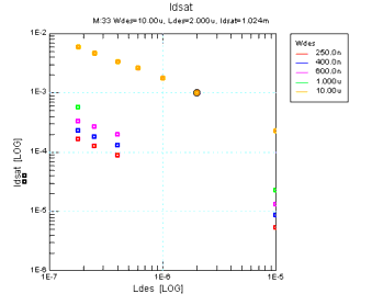
| • | Select one of the available plots and use the Plots > ZoomPlot > SelectedPlot menu item to see a zoomed display of the saturation current of all measured devices, for example. The plot to be displayed should look similar to the one shown below. For an explanation of this consistency check feature, see Consistency Check of DC measurement data for multiple measured devices. |
A check for the consistency of measured data can be activated by choosing Configuration > Check Data Consistency. This check is only possible when the Measurement subfolder is selected in the tree view. You will get a message if the rules of strict consistency are observed, otherwise you will get an error message. See Consistency Check of DC measurement data for multiple measured devices for details.
If the Device List subfolder is activated, you can check the DUT configuration by selecting Configuration > Check DUT Configuration from the menu. A window opens up to show misconfigured devices in detail. You can dump the contents of this window to the IC-CAP status window for reference.
Capacitance
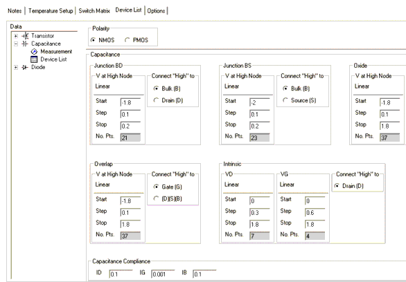
Click on the + sign in front of Capacitance in the tree view to open the Measurement definitions and the Device List for preparing capacitance measurements. Select Measurement to enter the polarity of the device, the measuring voltages and connections of the instrument as shown in Figure 19.
Figure 19 Capacitance measurement definitions
Physically Connecting Test Structures to your Capacitance Measurement Device
The following figure shows how to connect the CV instrument to measure oxide and overlap capacitances. See also the paragraph on test structures for CV measurement. In Table 67 you'll find recommended test structures for specific capacitances to be measured together with recommended instrument connections.
Figure 20 Measurement of oxide and overlap capacitance
The following figure shows a typical gate-to-drain/source overlap capacitance diagram that you would expect to measure with this type of connection and the default values for Start, Step, and Stop voltage VG.
To correctly extract overlap capacitance effects, two devices are essential: Standard CV measurement masks the channel capacity in short channel devices. This is the so called Short Channel Effect.
To overcome this masking, you need a short channel device for proper extraction of overlap capacitance parameters. To extract the parameter NGATE, you need to measure a long channel device in inversion since there is no short channel effect present in such a device.
Note
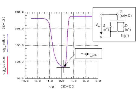
Figure 21 Example diagram of measured overlap capacity
Test Structures for CV Measurements
See Table 67 for a table of recommended test structures for CV measurements.
Capacitance Device List
Click on Device List to define the devices to be measured and their respective geometries. See the following cut out for an example.
This folder provides fields to enter names of DUTs, geometries and switch matrix connections, and to select temperatures at which to measure the DUTs.
| • | To add new DUTs: Choose the Add icon. You will be prompted for a group of capacitances to add DUTs to. Select the desired category (junction bulk-drain or bulk-source, oxide, overlap, or intrinsic) and choose Add. New lines are added according to the selection you made. |
Selecting overlap capacitances actually adds two DUTs: Overlap_GDS and Overlap_GDSB. For proper parameter extraction, you are required to measure both DUTs and extract the parameters from both measurements. Therefore, it only makes sense to add those DUTs together.
Since oxide capacitance requires only one test structure, you are able to have only one oxide capacitance DUT.
Note
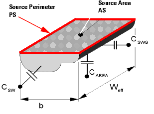
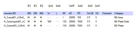
For each line, you can change the predefined name for the DUT and enter necessary geometrical data. For your convenience, only relevant data should be entered for a specific group of capacities. Relevant data fields are shown with white background and can be edited. Gray shaded data fields are not editable. For example, DUTs to measure bulk-drain junction capacitances do not require gate length and width (L, W), source area (AS) and perimeter length of source (PS) geometrical data. You only have to provide drain area (AD) and drain perimeter (PD) as well as the number of device fingers (NF) of the transistor to be measured. See Figure 22 for some details on capacitances and geometries.
W, AD, AS, PD, and PS are total values including all fingers of the device!
Note
Usually, you use single finger transistors for DC measurements. Multifinger devices are common only in high frequency characterization of MOS devices, since the input resistance of a network analyzer is typically 50 Ohm.
Note
Remember, all geometries are to be given in microns (µm).
Depending on your choice of temperatures on the Temperature Setup folder, one or more columns are marked with the temperatures you have entered appear. The fields of those columns show either (0) for no measured data available, (M) for DUT already measured or (-) for DUT not to be measured at that temperature.
You can enter a comment for each DUT. When using a switch matrix for capacitance measurements, you can enter a module name to measure one complete module with all its DUTs at once. This is intended for use with a prober card and taking measurements using the "step and repeat" function of a wafer prober. If you are using a switch matrix, you must enter the pin numbers of the switch matrix pin connections to the capacity you`re about to measure. The fields for high and low connection of the CV measuring instrument are marked H or L respectively, the ground connection is to be entered in the column marked 0. Since a ground connection is not required for every measurement, only those fields where a ground connection is not required are marked with a "-", all others are predefined to node No. "0". See Test Structures for CV Measurements for details on device geometries and requirements for proper extraction of capacitances of your devices like test lead connections and so on.
| • | To delete DUTs: Choose the Delete icon or Delete from the Configure menu. You will be prompted with a list of DUTs. Select the DUTs to be deleted and choose Delete on the Delete DUT folder. A prompt dialog box appears. Select OK if you are satisfied with your choice of DUTs to be deleted. |
| • | To select devices to be measured at different temperatures: Choose the Temperature Measurement icon or Temperature Measurement from the Configuration menu. You will be prompted with a list of DUTs. Select the devices to be measured at those temperatures entered in the Temperature Setup folder and click OK. |
You cannot prevent a DUT from being measured at TNOM. All DUTs are measured automatically at that temperature. If you have entered one or more temperatures on the Temperature Setup folder, the DUTs selected for temperature measurement are all measured at those temperatures. In other words, you cannot select a DUT for measurement at temperature T1 but not at another temperature T2.
Note
| • | To start measurement of the devices: Choose the Measure icon and select the DUTs to be measured on the dialog box that opens. You can select measurement temperature (if there is a temperature other than TNOM defined in the Temperature Setup folder) as well as a specific DUT or all DUTs. Start the measurement with Measure on that dialog box. If measuring at elevated temperatures, be sure to wait until your devices are heated up or cooled down to the desired temperature. |
| • | If you would like to clear some or all measured data, choose Clear Data from the Data menu. You can select whether you would like to clear measured data of some or all DUTs at specified temperatures and click Clear Data to delete measured data files. |
| • | Using Synthesize Measured Data from the Data menu, you can simulate capacitance data from existing parameters. These synthesized data use the voltages set on the Measurement Conditions folder to generate "measurement" data from a known set of SPICE parameters. It might be especially useful to convert parameters of other models into BSIM3 or BSIM4 parameters by loading the created "measurement data" into the extraction routines and extract parameters for the desired model. |
| • | To see the diagrams of what has just been measured, click the Display Plots icon. You will see a dialog box to select which measured data set you would like to display. After choosing the plots you would like to see, click Display Plots on that dialog box to open the selected plots. This is a convenient way to detect measurement errors before starting the extraction routines. |
| • | If you are satisfied with the data you have just measured, choose Close Plots to close the windows that show diagrams of measured data. |
Diode
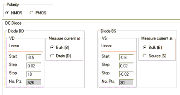
This part of the Data tree is used to define measurements for Junctions/Diodes of the devices to be measured. First, define the measurement conditions to reflect the desired voltages, Number of Points, and Compliances used for the measurement.
Next, select the Device List to enter names of DUTs, geometries and switch matrix connections, and to select temperatures at which to measure the DUTs. Don't forget to Save your setup after you've entered the DUT data. Table 66 briefly describes usable test structures to characterize diode behavior.
| • | To add new DUTs: Click the Add icon. You will be prompted with a list to select DUTs to add. Select the desired DUTs and click Add. New lines are added according to the selection you've made. |
If you have entered all necessary categories, clicking Add will not open a window to select new diode DUTs, since all are present. Measuring more diode DUTs will not create new information, since the measured values will be the same as the one's that have been measured already.
Note
For each line, enter a name for the DUT and necessary geometrical data. For your convenience, only relevant data is to be entered for specific diodes. Relevant data fields have a white background, irrelevant data fields show a dashed line. For example, DUTs to measure bulk-drain diodes do not require source area (AS) and perimeter length of source (PS) geometrical data. You only have to enter drain area (AD) and drain perimeter (PD) as well as the number of device fingers (NF) of the diode to be measured. Remember, all geometries are to be given in microns (µm).
W, AD, AS, PD, and PS are total values including all fingers of the device!
Note
Depending on your choice of temperatures on the Temperature Setup folder, one or more columns marked with the temperatures you have entered appear. The fields of those columns show either (0) for no measured data available, (M) for DUT already measured or (-) for DUT not to be measured at that temperature.
| • | You can enter a comment for each DUT. If you are using a switch matrix, you can enter a module name as well as the pin numbers of the switch matrix pin connections to the transistor. Only relevant connections should be entered. In the case of the bulk-drain diode, no source connection should be entered (the appropriate field shows a dashed line). See Figure 22 for details on device geometries and Table 68 for requirements on a proper extraction of diode data. |
| • | To delete DUTs: Choose Delete from the icons or menu. You will be prompted with a list of DUTs. Select the DUTs to be deleted and click Delete on the Delete DUT folder. A prompt dialog box appears. Choose OK if you are satisfied with your choice of DUTs to be deleted. |
| • | To select devices to be measured at different temperatures: Choose Temperature Measurement from the Configuration menu. You will be prompted with a list of DUTs. Select the devices to be measured at the temperatures entered in the Temperature Setup folder and click OK. |
You cannot prevent a DUT from being measured at TNOM. All DUTs are measured automatically at that temperature. If you have entered one or more temperatures on the Temperature Setup folder, the DUTs selected for temperature measurement are all measured at those temperatures. In other words, you cannot select a DUT for measurement at temperature T1 but not at another temperature T2.
Note
| • | To start measurement of the devices: Click the Measure icon and select the DUTs to be measured on the dialog box that opens. You can select measurement temperature (if there is a temperature other than TNOM defined in the Temperature Setup folder) as well as a specific DUT. Start the measurement with Measure on that dialog box. If measuring at elevated temperatures, be sure to wait until your devices are heated or cooled down to the desired temperature. |
| • | If you would like to clear data of some or all measured DUTs, use Clear Data from the Data menu. Select whether you would like to clear measured data of some or all DUTs at specified temperatures, and click Clear Data to delete measured data files. |
| • | Using Synthesize Measured Data from the Data menu, you can simulate data from existing parameters. This synthesized data uses the voltages set on the Measurement Conditions folder to generate "measurement" data from a known set of SPICE parameters. |
| • | To see the diagrams of what has just been measured, use the Display Plots icon. You will see a dialog box to select which measured data set you would like to display. Choosing the plots you would like to see, opens the selected plots. This is a convenient way to detect measurement errors before starting the extraction routines. |
| • | If you are satisfied with the data you just measured, use the Close Plots icon to close the windows that show diagrams of measured data. |
Drain/Source – Bulk Diodes for DC Measurements
For test structures to measure DC Drain/Source-to-Bulk diodes, see Drain/Source – Bulk Diodes for DC Measurements.
Options
This folder lets you define options for the appearance of the plot windows.
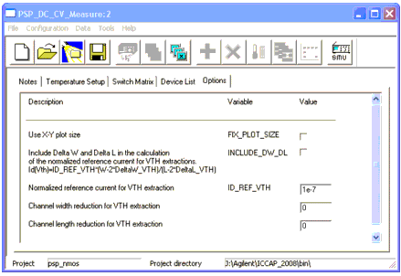
To change the plot window size, deselect the FIX_PLOT_SIZE.
To change the background color of a plot window, in the plot window select Options > Exchange Black-White. This changes a white background to black or a black background to white.
You can select if you want to include Delta W and Delta L into the VTH extraction process.
You can also set a value for the normalized reference current, as well as Channel width and length reduction values for VTH extraction. Those values should be entered as a dimension in meters.
Import Wizard
This feature enables you to import data measured using data formats or software not compatible with the IC-CAP format. The base for this task are project description files in spreadsheet format (.csv files). As a template for these csv files, the File > Export menu contains selections to create devices lists for DC, Capacitance, and Diode data. Load a project into the IC-CAP Measurement module, then select either DC device list, Capacitance device list, or Diode device list. A csv style file will be created. This file can be opened with EXCEL, for example. It contains all device data that was entered into the DC, Capacitance, or Diode DUTs folder.
You can edit the project document or you can create a new one using the same format. The first row of the sheet contains keywords. The values below these keywords will be read into IC-CAP and are assigned to the appropriate values in the MOS Modeling Toolkits. By default, the list contains a certain set of keywords. However, you can add more keywords to help define the import paths. All keywords can be used later to describe the name and the location of the stored .mdm file.
The Role of the MDM_FILE_CONSTRUCTOR
The major problem in accessing raw .mdm data is that there are many possible data organization schemes. The mdm files can be sorted according to the temperature in different directories and in one directory per device and so on.
To cover these different solutions, the MDM_FILE_CONSTRUCTOR is introduced. Its purpose is to enable you to define the mdm file structure. This is done using the different keywords from the device list files and the import GUI.
Functionality
The import routine performs the following steps:
- According to the definition in the MDM_FILE_CONSTRUCTOR, the import routine looks for all available files first, which are described by this expression. Let's assume that the MDM_FILE_CONSTRUCTOR looks like
<DIR>
<DEVICE_NAME>
<TEMP_ALIAS>
<MDM-FILE>
C:\tmp
Transistor_1
minus40
idvg
Transistor_2
25
idvd
Transistor_3
125
my_idvg
- In this case, all possible combinations using the 4 keywords are generated, and each combination is then checked as to whether or not the file exists.
- In the second step, the existing files are imported to IC-CAP. The necessary device information (L, W, e.t.c.) is taken from the device list and is added to the file. Furthermore, different checks are performed to make sure that the file is correct. If necessary, settings are corrected or added. In particular, these are:
| • | node numbers (G is associated to vg, e.t.c.) |
| • | name of inputs (vg must be in lower case) |
After these modifications, the files are saved in the new project directory.
Example Export/Import Procedure
Export a csv Sheet as a Template
Open the DC_CV_Measurement module using the model you would like to import data into (e.g., BSIM4_DC_CV_Measure). Open a project (e.g., BSIM4_for_experts). Choose File > Export > DC device list (or Capacitance device list or Diode device list). A window opens for you to enter the name and path for the file. Once the entries are made, click Save. A .csv file will be saved with the specified name and path. The following figure shows the file.
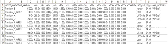
Figure 25 Via Export generated csv sheet
You can edit the template to suit your specific needs (e.g., dimensions, device names, and so on).
Import Data into the BSIM4 MOS Modeling Package
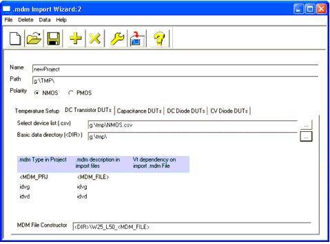
After adapting the template to your project, select File > Import > Import Wizard (.mdm). The mdm Import Wizard window opens and the "Model"_DC_CV_Measure window is temporarily closed. Select File > New from the wizard, browse to the location where you want to store the project, and enter a name for your project. Select Create.
On the Temperature Setup folder, enter TNOM in Kelvin and, if used, a temperature alias. If you have data measured at other temperatures, add those temperatures as well.
Next, open the DC Transistor DUTs folder, select the desired device list as well as the Basic data directory, then enter the MDM_FILE_CONSTRUCTOR into the line at the bottom of the window (see the following figure). Don't forget to enter the correct .mdm description in import files assignment. Check the entries by clicking the Assignment icon ![]() to check the input/output assignment.
to check the input/output assignment.
Correct, if necessary.
In the following example, the files in the Import Wizard window are located in G:\tmp and are named W25_L50_idvg.mdm respective W25_L50_idvd.mdm.
When all folders are filled with the required information, start the automatic checking process by clicking ![]() . The Import check window appears—see below.
. The Import check window appears—see below.
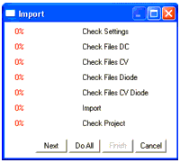
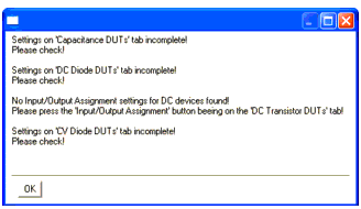
You can check each setting step-by-step using the Next button or you can Do All checks automatically. You will get error messages if something is wrong.
If no errors occur, the Finish button on the Import window will be activated. Press this button to complete the import process before saving the changes and exiting the wizard. The DC_CV_Measure GUI opens again and the project just created is now ready to open.