Print version of this Book (PDF file)
Test structures for Deep Submicron CMOS Processes
A very important prerequisite for a proper model parameter extraction is the selection of appropriate test structures. The following sections describe the necessary test structures for the determination of CV and DC model parameters. A very detailed description of ideal test structures can be found in the JESSI AC-41 reports [2].
Transistors for DC measurements
The minimum set of devices for a proper extraction of DC model parameters is marked with ![]() in the following figure. This means one transistor with large and wide channel (and therefore showing no short/narrow effects), one transistor with a narrow channel, one transistor with a short channel, and one device with both short and narrow channel. Please note that with this minimum set of devices some parameters cannot be determined correctly (see the chapter "Extraction of parameters") and they are set to default values during the extraction. For an extraction of all model parameters and a better fit of the simulated devices over the whole range of designed gate length and gate width, use more devices with different gate lengths and gate widths as shown in the following figure with
in the following figure. This means one transistor with large and wide channel (and therefore showing no short/narrow effects), one transistor with a narrow channel, one transistor with a short channel, and one device with both short and narrow channel. Please note that with this minimum set of devices some parameters cannot be determined correctly (see the chapter "Extraction of parameters") and they are set to default values during the extraction. For an extraction of all model parameters and a better fit of the simulated devices over the whole range of designed gate length and gate width, use more devices with different gate lengths and gate widths as shown in the following figure with ![]() signs. You can use additional devices, for example, for evaluating the extraction results for certain channel lengths and widths used in your process. They are marked
signs. You can use additional devices, for example, for evaluating the extraction results for certain channel lengths and widths used in your process. They are marked ![]() .
.
Figure 135 Recommended Test Transistor Geometries for proper parameter extraction
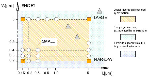
a) Requirements for Devices
Large
- For a proper extraction of the basic model parameters, the short and narrow channel effects should not affect the large device extraction. Also the drain-source-resistance parameters should not have an influence on the simulated behavior of the large device. For a typical 0.5 micron CMOS process with a gate oxide thickness of 11 nm, a large device with channel length of 10 microns and channel width of 10 microns was found to meet these requirements.
- You can check this prerequisite if you only extract the parameters in the idvg/Large setup and then perform a simulation of the setup idvg/Large_m. After that simulation, perform the other geometry extractions and re-simulate the idvg/Large setup again. Now, the curve ID = f(Vgs) should not change more than roughly 5% compared to the first simulation. If the difference is bigger, a larger device should be used to enable a good extraction of the basic model parameters.
- You can check this prerequisite if you only extract the parameters in the idvg/Large setup and then perform a simulation of the setup idvg/Large_m. After that simulation, perform the other geometry extractions and re-simulate the idvg/Large setup again. Now, the curve ID = f(Vgs) should not change more than roughly 5% compared to the first simulation. If the difference is bigger, a larger device should be used to enable a good extraction of the basic model parameters.
Narrow
- For the DUT Narrow_m you should use a device with the smallest designed gate width of your process. Using more narrow devices will increase the number of parameters that can be extracted and will lead to a better fit of the curves over the range of different channel widths.
Short
- For the DUT Short_m you should use a device with the shortest designed gate length of your process. Using more short devices will increase the number of parameters that can be extracted and will lead to a better fit of the curves over the range of different channel lengths.
Small
- For the DUT Small_m you should use a device with the shortest designed gate length and the smallest designed gate width of your process. This small device will incorporate all short and narrow channel effects and will be an indicator of how good your parameter extractions are.
In general
- It is recommended to use the designed gate lengths and widths. Effects due to under diffusion or decrease of poly-Si gate length are sufficiently covered by the extraction routines and the model itself.
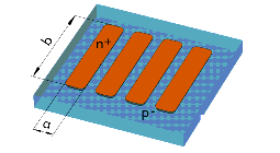
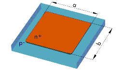
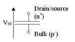
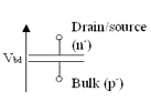
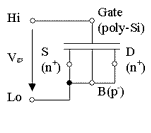
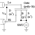
Drain/Source – Bulk Diodes for DC Measurements
Test Structures for CV Measurements
The following table provides example test structures for measuring capacitance-voltage properties. Each test structure includes a description as well as a schematic for setting up the measurements. You can modify these examples by changing the low and high connection of the CV meter.


Testchips
- You will find an example for a test chip design, which meets most of the requirements of the extraction of BSIM3v3 model parameter, in the JESSI Report AC 41 94-3 "Description of parametrized European Mini Test Chip." Please check also the test chip design of the Fabless Semiconductor Association in the U.S. (http://www.fsa.org).
Test Structures for S-parameter Measurements
a) Test Structures
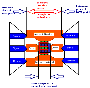
Performing S-parameter measurements with MOS devices on a wafer requires properly designed test structures that meet certain requirements:
| • | The test devices must drive enough current for correct measurement results |
| • | They should fulfill the specifications for high frequency probes |
| • | Additional structures should be available for the measurement of parasitic elements to de-embed them from the measurements on the test device |
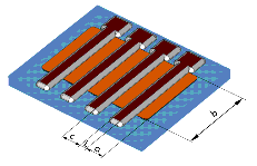
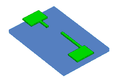
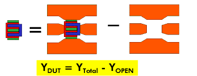
A principle layout of such a test structure is shown in the following figure [9].
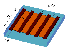
Figure 136 Layout of a Test Structure for a MOS Transistor
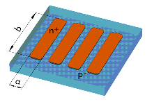
The MOS transistor is designed as a finger structure with four common gates, three source areas and two drain areas. In summary, this compact layout results in a very wide gate width, which can drive a high current Ids.
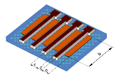
The probes are connected in a Ground-Signal-Ground scheme according to the recommendations in [4]. As it is shown above, the calibration plane of the network analyzer is at the end of the probe head. This means, the transmission lines that connect the DUT with the probe head must be modeled and their effect must be de-embedded from the measured data of the DUT. This can be done by measuring an OPEN and a SHORT test device without a DUT and using these measurements to de-embed the parasitic influence of the pads. The following two figures show the design of these OPEN and SHORT test structures. Both of these test structures will be used for a simple and effective de-embedding procedure (OPEN_SHORT) as will be shown later. Additional test devices, like a THROUGH device can be used to verify the de-embedding strategy. In general, the complexity of the de-embedding procedure depends on the frequency range of the measurements and the design of the test structures. However, a proper de-embedding is the absolute pre-requisite for an accurate AC modeling of the MOS transistor.
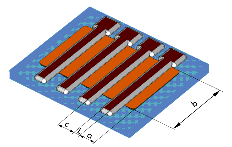
Figure 137 OPEN, SHORT and THROUGH structure without MOS transistor


b) De-embedding procedures
The DUT Deembedding > Calculation contains five different setups, two for general purposes and three with different de-embedding methods, to be selected depending on the availability of test structures and the frequency range of measurements. They are:
| • | no_deembedding |
| • | resetDeembedding |
| • | deembed_open |
| • | deembed_open_short |
| • | deembed_user_defined |
1. OPEN:
This the simplest way of de-embedding and is often used for frequency ranges up to 10 GHz. It is assumed that the parasitics can be modeled using the following equivalent circuit:
Figure 138 Equivalent circuit for the parasitic elements (including MOS-Transistor)

The OPEN device is measured and the S-parameters of the DUT are calculated as shown next:
Stotal -> Ytotal, Sopen -> Yopen
Ydut -> Sdut
- Stotal -> measured S-parameters of the DUT including parasitics
- Sopen -> measured S-parameters of the OPEN test structure
- Sdut -> S-parameters of the DUT without influence of the parasitics
- Yxxx -> transformed Y-parameters with:
- 'Ytotal = TwoPort(Stotal,"S","Y")'
- Sopen -> measured S-parameters of the OPEN test structure
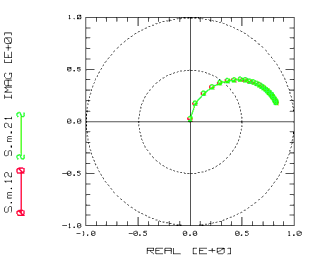
The typical behavior of this test structure is shown in the following 2 figures.
Figure 139 S11,22 of the OPEN structure
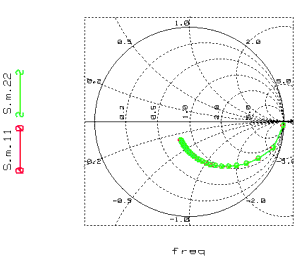
Figure 140 S12,21 of the OPEN structure
2.OPEN_SHORT:
This is a very fast and effective way of de-embedding from measurements of an OPEN and a SHORT device. It is useful for frequencies above roughly 3.5 GHz if the accuracy of the OPEN method is not satisfying.
This method is described in detail in the IC-CAP demo_features. (See the file: $ICCAP_ROOT/examples/demo_features/4extraction/ deemb_short_open.mdl)
It is assumed that the parasitics can be modeled using the following equivalent circuit:
Figure 141 Detailed equivalent circuit of MOS-Transistor

The transistor is located between nodes: Gate = 222, Drain = 111, Source, Bulk = 333
Regarding the two test structures OPEN and SHORT and their equivalent circuits, it is assumed that there are ONLY parallel parasitics followed by serial parasitics. If this pre-requisite is valid, the measured data of the SHORT device and the measured data from the DUT have to be de-embedded from the outer parallel parasitic elements first (after a conversion of S to Y parameters):
The subsequent step is to de-embed the measured data of the DUT from the serial parasitic elements and convert them back to S-parameters:
The typical behavior of the OPEN_SHORT structure is shown in the two figures below:
Figure 142 S11,22 of the OPEN_SHORT structure
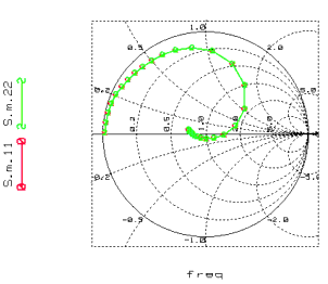
Figure 143 S12,21 of the OPEN_SHORT structure
3.USER_DEFINED:
This setup can be used to implement user-specific de-embedding procedures with other test structures than OPEN and SHORT or to achieve a higher quality in de-embedding.
Please see the transform deembed_all to locate the entry point for your specific de-embedding procedure.
The ultimate tool for de-embedding with IC-CAP is the De-embedding Tool-kit where a large number of ready-to-go solutions together with the theoretical background can be found. Please contact Dr. Franz Sischka from Agilent EEsof (franz_sischka@agilent.com) for more details.
c) Verification procedures
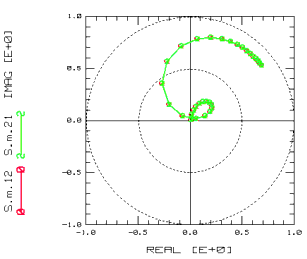
The BSIM3v3 Modeling Package provides a method to verify the de-embedding. It uses a THROUGH dummy test device. After a correct de-embedding of the parasitic components, the S-parameters of the THROUGH should show the behavior of an ideal, matched transmission line with Z0=50 Ohm and a TD that represents the electrical length of the through line in the THROUGH dummy device.
The S11 and S22 curve should be concentrated in the center of the Smith chart, while S21 and S12 should both begin at (1+j*0) and turn clockwise on the unity circle.
If these pre assumptions are not given, the following items should be checked:
| • | Is the calibration OK? |
| • | If the OPEN method is used, consider to enhance the de-embedding quality by using the OPEN_SHORT method, which removes the inductive parasitics in the measured data. |
| • | If the OPEN_SHORT method is used and the frequency is very high (>30 GHz), it should be checked whether the assumptions for using OPEN_SHORT are still given. The easiest way to do this is to model the OPEN and the SHORT device using the equivalent circuits given in Test_open and Test_short. |
Physical Length Verification of the Through Test Structure
Checking the physical length of the Through line involves a measurement of the phase angle between the input and output signal of the through. Since it is assumed that the through line is designed to give a Z0 of 50 Ohms (as is used for RF measurements using a network analyzer), the output and input signal amplitude are the same. The S-parameter measurement gives a phase difference between input and output signals. Using the Smith diagram, you can calculate the physical length of the through line between the pads using the phase difference of the signals. This phase difference ![]() is calculated from:
is calculated from:
![]() = length of the line (distance between pads)
= length of the line (distance between pads)
Since ![]() , the electrical length of the line is
, the electrical length of the line is
The formulas above are valid only for air as dielectricum, since the velocity of the wave depends on the relative dielectric and permeable constants of the material. Building standard test structures on silicon wafers using silicon dioxide as dielectric, changes the propagation velocity of the waves from light speed (c) to:
The constants for silicon and silicon dioxide are:
Material
![]()
![]()
Silicon
1
11.8
Silicon dioxide
1
3.9
Typically, the test structures are built on a silicon wafer on top of the silicon dioxide isolator. This leads us to a propagation velocity of:
Using this result, the physical length of the line would be:
Example
A measurement gives a phase difference between input and output of a through line as 10° at a frequency of 5 GHz. The test structure uses silicon dioxide as the isolator material. We would like to know the electrical length of our through test structure. Using the above formula leads to:
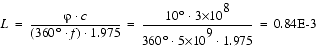
Therefore, the physical length of the measured line is 0.84E-3 m or 840 µm.