Print version of this Book (PDF file)
DC Behavioral Modeling
This section provides a theoretical background of the BSIM4 DC model. You will find some basic device equations together with some explanations on model selectors used inside the BSIM4 model and the BSIM4 Modeling Package.
At the end of this section you will find a table listing all of the model parameters added in BSIM4.3.0 together with their default values as well as a table containing the parameter set used in version BSIM4.2.1.
Since this theoretical section can only be of introductional character, we strongly recommend that you consult the manual from the University of California, Berkeley for a detailed description of device equations and relevant parameters [1] as well as further literature located in References.
Threshold Voltage Model
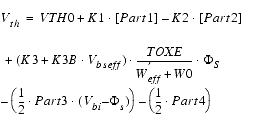
The complete threshold voltage model equation implemented in the BSIM4 model for SPICE is (the influence of the well-proximity effect is described at the end of this paragraph):
The equation above contains some shortcuts for better readability (![]() ). Expanded they read:
). Expanded they read:
To set an upper boundary for body bias during simulations, the effective body bias has been introduced:
where ![]() and
and ![]() is the maximum allowable
is the maximum allowable ![]()
Furthermore, there are some shortcuts used to make Equation 4 more readable.
- built-in voltage of the Source/Drain regions:
- effective channel length and width, ![]() and
and ![]() :
:
Well-Proximity effect modeling
With BSIM4.5.0, the calculation of influences from the so called well-proximity has been introduced. Deep buried layers, possible by using high-energy implanters, affect devices located near the mask edge. Ions, scattered at the edge of the photo resist film, can influence the threshold voltage of those edge devices. A threshold voltage shift in the order of around 100 mV have been observed [1]. The following figure shows the effect [7].
BSIM4.5.0 considers the variations of threshold voltage, mobility, and body effect through newly introduced parameters SCA, SCB, SCC, SC, WEB, WEC, KVTH0WE, K2WE, KU0WE, SCREF, and WPEMOD.
The relevant model equations are:
The following sections provide equations for effects modeled in the complete equation above, Equation 4. Starting from the basic equation for long and wide channels, the effects of shrinking dimensions and substrate doping variations are modeled step by step.
Basic Threshold voltage equation
For long and wide channels the following equation is valid:
Equation 6 is valid under the following assumptions:
| • | constant substrate (channel) doping |
| • | long and wide channel |
Model parameters used for the equation above are listed in the table below:
If the substrate doping is not constant or if the channel is short and/or narrow, the basic equation should be modified. The following sections show modifications to the basic equation for non-uniform doping concentration and for short or narrow channel effects.
Non-Uniform Substrate Doping
If the substrate doping concentration is not uniform in vertical direction, the body bias coefficient ![]() is a function of the substrate bias and the depth from the interface. The threshold voltage in case of non-uniform vertical doping is:
is a function of the substrate bias and the depth from the interface. The threshold voltage in case of non-uniform vertical doping is:
The doping profile is assumed to be a steep retrograde and is approximated in BSIM4. For details on how it is modeled, see the manual from UC Berkeley [1] starting on page 2-2. The model parameters K1 and K2 can be calculated from NSUB, XT, VBX, VBM, and so on. This is done the same way as in BSIM3v3. Details can be found on page 2-4 of the BSIM4 manual.
ni
intrinsic carrier concentration in the channel region
PHIN
PHIN
Non-uniform vertical doping effect on surface potential
0.0
Non-Uniform Lateral Doping: Pocket or Halo Implant
The doping concentration in this case varies from the middle of the channel towards the source/drain junctions. Shorter channel lengths will result in a roll-up of ![]() from the rise of the effective channel doping concentration and the changes of the body bias effect. Those effects are considered using the following formulation:
from the rise of the effective channel doping concentration and the changes of the body bias effect. Those effects are considered using the following formulation:
Additionally, drain-induced threshold shift (DITS) has to be considered in long-channel devices using pocket implant. For ![]() in a range of interest, a simplified threshold voltage shift caused by DITS was implemented:
in a range of interest, a simplified threshold voltage shift caused by DITS was implemented:
Using TEMPMOD=2, this formula changes to
Short-Channel and Drain-Induced-Barrier-Lowering (DIBL) Effects
For shorter channels, the threshold voltage is more sensitive to drain bias (DIBL effect) and less sensitive to body bias because of reduced control of the depletion region.
The short channel effect coefficient is given by
In BSIM3v3 this equation is approximated, which results in a phantom second roll-up when Leff becomes very small. To avoid this effect, the exact formulation is used in BSIM4. Model flexibility is increased for different technologies with additional parameters introduced and the short-channel and drain-induced-barrier-lowering effects are modeled separately.
This leads to a short-channel effect coefficient of the form:
and a variation of Vth due to the short-channel effect of:
Drain-induced barrier lowering is modeled the same way, the threshold voltage shift due to DIBL is calculated as:
DVT1 is basically equal to 1/( )1/2, ETAB and DVT2 represent the influence of substrate bias effects on SCE and DIBL.
Narrow-Width Effect
The existence of fringing fields leads to a depletion region in the channel that is always larger as is calculated using one-dimensional analysis. This effect gains more influence with decreasing channel widths since the depletion region underneath the fringing field becomes comparable to the depletion field formed in vertical direction. The result is an increase of Vth.
The formulation for the narrow-width effect is:
Subthreshold Swing
In the subthreshold region, the drain current flow is modeled by:
The expression ![]() represents the offset voltage and
represents the offset voltage and
gives the channel current at ![]() .
.
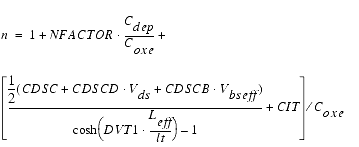
The subthreshold swing parameter n is determined by channel length and interface state density and is calculated using
The parameter NFACTOR is used to compensate for errors in calculating the depletion width capacitance.
Gate Direct Tunneling Current Model
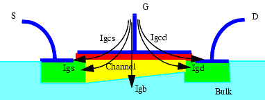
Gate oxide thickness is decreasing, therefore tunneling currents from the gate contact are playing an important role in the modeling of sub micrometer MOSFET's. In BSIM4, the gate current consists of one part tunneling from gate to bulk (Igb) and one part tunneling from gate to channel (Igc). The latter one again is partitioned to flow to the source contact (Igcs) and to the drain contact (Igcd), as well as from the gate to the source and drain diffusion regions (Igs, Igd), as is shown in the following figure.
Figure 58 Cross section of a MOSFET with gate tunneling current components
Two model selectors are used to turn on or off tunneling current components, IGBMOD and IGCMOD. Setting IGBMOD = 1 turns on Igb, IGCMOD = 1 turns on Igc, Igs and Igd. Setting IGBMOB = IBGCMOD = 0 turns off modeling of gate tunneling currents.
The BSIM4.3.0 Version of the model allows the modeling of Gate Current Tunneling through Multiple-Layer Stacks by use of a tunneling attenuation coefficient.
Gate-to-Bulk Current
This current consists of two parts, tunneling of electrons from the conduction band and from the valence band. The first part is significant in the accumulation region, the second one during device inversion. The accumulation region tunneling current is dominated by electron tunneling from the conduction band and is given by:
Inside this equation, the auxiliary voltage is:
The constants in this equation are:
The tunneling current dominating the inversion region is caused by electron tunneling from the valence band. It is calculated by:
Inside this equation, the auxiliary voltage is:
The constants in the above equation are:
The voltage across the gate oxide Vox consists of the oxide voltage in accumulation and the one in inversion, as used in Equation 17 and Equation 18.
The parts of Vox are calculated by:
The flatband voltage, calculated from zero-bias Vth is:
Equation 19 is continuously valid from accumulation through depletion to inversion.
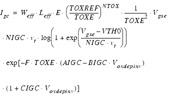
Gate-to-Channel Current Igc
The gate-to-channel current is determined by electrons tunneling from the conduction band in NMOS transistors respective holes tunneling from the valence band in PMOS transistors.
The physical constants E and F are listed in Table 41.
Gate-to-Source and Gate-to-Drain tunneling currents
These currents tunnel from the gate contact to the source or drain diffusion regions. They are caused by electron tunneling from the conduction band in NMOS transistors and by hole tunneling from the valence band in PMOS transistors.
For the computing of Igd, the values of Vgs in Equation 21 has to be replaced by Vgd.
The flat-band voltage between and the source or drain diffusion areas is dependent from NGATE:
To take drain bias effects into account, the tunneling current from the gate contact splits into two components and it is ![]() . The components are calculated as:
. The components are calculated as:
If the model parameter PIGCD is not specified, it is calculated by:
The constants used in Equation 21 and Equation 22 have different values for NMOS and PMOS transistors:
E
4.97232 A/V²
3.42537 A/V²
F
7.45669E11 ![]()
1.16645E12 ![]()
DLCIG
DLCIG
Source/Drain overlap length for Igs and Igd
LINT
POXEDGE
POXEDGE
Factor for gate oxide thickness in source/drain overlap regions
1.0
AIGSD
AIGSD
Parameter for Igs and Igd
NMOS: 0.43
PMOS: 0.31
BIGSD
BIGSD
Parameter for Igs and Igd
NMOS: 0.054
PMOS: 0.024
CIGSD
CIGSD
Parameter for Igs and Igd
NMOS: 0.075
PMOS: 0.03 [V]
NIGC
NIGC
Parameter for Igcs, Igcd, Igs and Igd
1.0
PIGCD
PIGCD
Vgs dependence of Igcs and Igcd
1.0
Drain Current Model
Bulk Charge
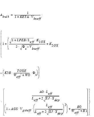
If a drain-source voltage other than zero volts is applied, the depletion width along the channel will not be uniform. Therefore, the threshold voltage VTH will vary along the channel. This phenomenon is known as the Bulk Charge Effect. Inside BSIM4, the bulk charge effect is formulated as follows:
Abulk is about 1 for small channel lengths and increases with increasing channel length.
Note
Unified Mobility Model
Mobility of carriers depends on many process parameters and bias conditions. Modeling mobility accurately is critical to precise modeling of MOS transistors. BSIM4 provides three different mobility models, selectable through the MOBMOD flag. The MOBMOD = 0 and 1 models are the same as being used in BSIM3v3. There is a new and accurate universal mobility model, selectable through MOBMOD = 2, which is also suitable for predictive modeling [1].
With BSIM4.5.0, an Leff dependency was added to the formulas for the effective mobility using the newly introduced parameters UD and UP (see parameter list for details).
MOBMOD = 0:
MOBMOD = 1:
MOBMOD = 2
The constant C0 has different values for different MOS processes. For NMOS processes C0 = 2, for PMOS processes C0 = 2.5 is used.
Using UD = 0.0 and UP = 0.0, the model is backwards compatible.
Drain/Source Resistance Model
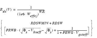
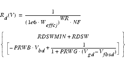
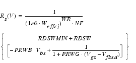
The resistances of the drain/source regions are modeled using two components: The sheet resistance, which is bias-independent, and a bias-dependent LDD resistance.
In contrast to the BSIM3 models, the drain and source LDD resistances are not necessarily the same, they could be asymmetric. This is a prerequisite for accurate RF simulations.
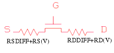
A further enhancement of the BSIM4 model over BSIM3 is the external or internal RDS option, invoked by the model selector RDSMOD = 0 (internal RDS) or RDSMOD = 1 (external RDS). The external RDS option looks at a resistance connected between the internal and external source and drain nodes. See the following figure.
RDSMOD = 0 (internal Rs(V))
RDSMOD = 1 (external Rd(V) and Rs(V))
The flatband voltage Vfbsd is calculated as follows:
Saturation Region Output Conductance Model
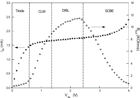
The following figure shows a typical MOSFET Ids vs. Vds diagram. The calculated output resistance is inserted into the diagram as well. This output resistance curve can be divided into four distinct regions, each region is affected by different physical effects. The first region at low Vds is characterized by a very small output resistance. It is called the linear region, where carrier velocity is not yet saturated.
Increasing Vds leads to a region that is dominated by carrier velocity saturation; this is the so-called saturation region. In this region, three different physical mechanisms are controlling device behavior. Those mechanisms are Channel Length Modulation (CLM), Drain-Induced Barrier Lowering (DIBL), and Substrate-Current Induced Body Effect (SCBE). Each of those mechanisms dominate the output resistance in a specific region.
Figure 59 Output Resistance vs. Drain-Source Voltage [1]
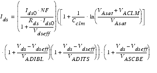
The continuous channel current equation for the linear and saturation region as implemented in BSIM4 is:
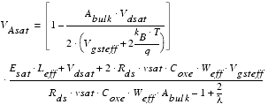
The Early voltage VAsat at ![]() is used to get continuous expressions for drain current and output resistance between linear and saturation region.
is used to get continuous expressions for drain current and output resistance between linear and saturation region.
In this equation, the channel current dependencies are modeled using specific Early voltages VA, as will be described in the following sections.
Channel Length Modulation - CLM
Through integration based on a quasi two-dimensional analysis, we obtain
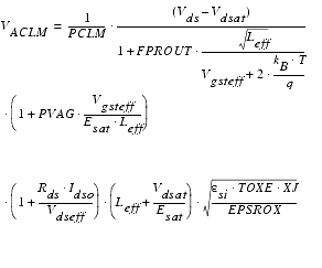
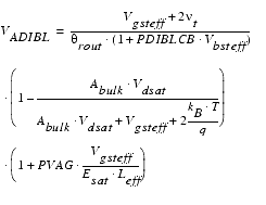
Drain-Induced Barrier Lowering - DIBL
The gate voltage modulates the DIBL effect. To correctly model DIBL, the parameter PDIBLC2 is introduced. This parameter becomes significant only for long channel devices.
The parameter ![]() is channel length dependent in the same manner as the DIBL effect in VTH, but different parameters are used here.
is channel length dependent in the same manner as the DIBL effect in VTH, but different parameters are used here.
Substrate-Current Induced Body Effect - SCBE
Due to increasing Vds, some electrons flowing from the source of an NMOS device will gain high energies and are able to cause impact ionization. Electron-hole pairs will be generated and the substrate current created by impact ionization will increase exponentially with the drain voltage. The early voltage due to SCBE is calculated by
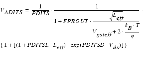
If the device is produced using pocket implantation, a potential barrier at the drain end of the channel will be introduced. The potential barrier can be reduced by the drain voltage even in long channel devices. This effect is called Drain-Induced Threshold Shift (DITS) and the early voltage due to DITS is
Body Current Model
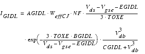
The substrate current of a MOSFET consists of diode junction currents, gate-to-body tunneling current, impact-ionization (Iii) and gate-induced drain leakage currents (IGIDL).
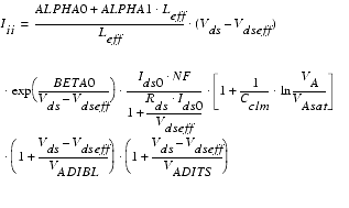
Impact Ionization Model
BSIM4 uses the same impact ionization model as was introduced in BSIM3v3.2. The impact ionization current is calculated by
Gate-Induced Drain Leakage
Stress Effect Modeling
The scaling of CMOS feature sizes makes shallow trench isolation (STI) a popular technology. To enhance device performance, strain channel materials have been used. The mechanical stress introduced by using these processes causes MOSFET performance to become a function of the active device area and the location of the device in the isolated region. Influence of stress on mobility and saturation velocity has been known since the 0.13 um technology [1].
For the named reasons, BSIM4 considers the influence of stress on:
| • | mobility |
| • | velocity saturation |
| • | threshold voltage |
| • | body effect |
| • | DIBL effect |
Mobility related dependence of device performance is induced through band structure modification. Doping profile variation results in Vth dependence of the stress effect. Both effects follow the same 1/LOD trend but have different L and W scaling influence. By modifying some parameters in the BSIM model, a phenomenological model has been implemented. The model assumes mobility relative change to be proportional to stress distribution.
Figure 60 MOSFET device geometry using a shallow trench isolation scheme
The figure above shows a typical MOSFET layout surrounded by shallow trench isolation. SA, SB are the distances between trench isolation edge to Gate-PolySi from one and from the other side, respectively. SD is the distance between neighboring fingers of the device. The Length of Oxide Definition (LOD) is expressed through the following equation:
2D simulation shows that stress distribution can be expressed by a simple function of SA and SB.
To cover doping profile changes in devices with different LOD, Vth0, K2, and ETA0 are modified.
The total LOD effect for multiple finger devices is the average of the LOD effect on every finger.
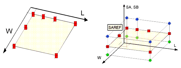
Since MOSFETs often use an irregular shape of their active area, additional instance parameters have to be introduced to fully describe the shape of the active area. This will result in many new parameters in the netlists and an increase in simulation time. To avoid this drawbacks, BSIM4.3.0 uses effective SA and SB values.
Figure 61 A "third" dimension is added to standard geometry parameters of MOSFET devices by introducing new parameters SA and SB to model stress effect influence on device performance
The left part of the figure above shows the geometry parameters used in MOSFET models so far. To the right, the SAREF-plane represents the standard L, W plane which is varied by SA and SB.
Until BSIM4.2.1, gate length (L) and gate width (W) have been the major device geometry parameters required.
For more details regarding the modeled stress effect influences on device performance, see Chapter 13 of the BSIM4.3.0 manual[1].
