Print version of this Book (PDF file)
The Unified I-V Model of BSIM3v3
For a complete summary of all equations of the BSIM3v3.2.4 model, please refer to the original documentation from University of California at Berkeley (see References to order this paper). The main equations of the BSIM3v3.3.0 model are shown together with a graphical representation for a better understanding of the model.
Please use the models BSIM3_DC_Tutorial.mdl, BSIM3_CV_Tutorial.mdl, BSIM3_AC_Noise_Tutorial.mdl, or BSIM3_Temp_Tutorial.mdl provided with the BSIM3 Modeling Package to visualize most of the model parameters influences onto the device diagrams. Load the file into IC-CAP to see how certain parameters affect the behavior of a deep submicron MOS transistor.
Threshold Voltage
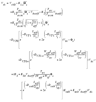
The threshold voltage is one of the most important parameters of deep submicron MOS transistors and is affected by many different effects when the devices are scaled down into the region of 0.1 microns. The complete equation of the threshold voltage in BSIM3v3.3.0 is given below.
The different parts of this complex equation are expressed by the following sub-equations in more detail:
Ideal Threshold Voltage
The basic equation of the threshold voltage is:
Vthideal
= ideal threshold voltage
VFB
= flatband voltage
 s
s = surface potential
ni
= 1.45 • 1010 (Tnom/300.15)1.5 (21.5566 - Eg0/2Vtmo)
Eg0
= 1.16 - 7.02 • 10-4 Tnom2/(Tnom + 1108)
This equation had been implemented into the first MOS simulation models assuming long and wide channels and uniform substrate doping. The following sections describe the effects that overlay this basic equation.
Non-Uniform Vertical Channel Doping
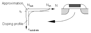
The substrate doping concentration N is not constant in the vertical direction of the channel, as shown in the following figure.
Figure 70 Vertical Doping Profile in the Channel
It is usually higher near the silicon to silicon dioxide interface than deeper in the substrate. This higher doping concentration is used to adjust the threshold voltage of the device. The distribution of impurity atoms inside the substrate is approximately a half Gaussian distribution, which can be approximated by a step function with NCH for the peak concentration in the channel near the Si-SiO2 interface and Nsub in the deep bulk. XT is the depth where the approximation of the implant profile switches from NCH to NSUB. The non-uniform vertical channel doping affects the threshold voltage when a bulk source voltage is applied to the device and is represented here as the part ΔVth(1) of the overall threshold voltage.
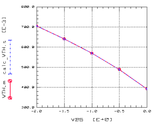
In BSIM3, either the model parameters K1 and K2 or NCH, NSUB, VBM or XT can be used to model this effect. The following figure shows the threshold voltage Vth as a function of the applied bulk voltage for a transistor with a large channel length and a wide channel width (LARGE).
Figure 71 Threshold Voltage Vth as a Function of Vbs
Non-Uniform Lateral Channel Doping
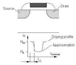
The doping concentration Nds near the drain and the source is higher than the concentration Na in the middle of the channel. This is referred to as lateral non-uniform doping concentration and is shown in the following figure.
Figure 72 Lateral Doping Profile in the Channel
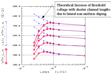
As the channel length becomes shorter, the lateral non-uniform doping will cause the threshold voltage to increase strongly because the average doping concentration in the channel becomes higher. This part of the threshold voltage is modeled with the parameter Nlx and is represented by ΔVth(2) as a part of the overall threshold voltage.
The following figure shows the influence of the non-uniform lateral doping on the threshold voltage as a function of gate length.
Figure 73 Threshold Voltage as a Function of Gate Length Due to Lateral Non-Uniform Doping
You can distinguish between the theoretical trace following Equation 55 and the real world ones with the short channel effect described in the next section.
Short Channel Effect
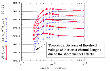
The threshold voltage of a long channel device is independent of the channel length and the drain voltage as it is shown in the equation of the ideal threshold voltage. The decreasing of device dimensions causes the so-called short-channel effects: threshold voltage roll-off and degradation of the subthreshold slope, that in turn increases the off-current level and power dissipation. The threshold voltage then depends on geometrical parameters like the effective channel length and the shape of the source-bulk and drain-bulk junctions. These device dimensions have a strong influence on the surface potential along the channel. A shallow junction with a weak lateral spread is desirable for the control of short-channel effects while the source and drain resistance must be kept as low as possible. However, a trade-off between the search for very shallow junctions and the degradation of the maximum achievable current through the parasitic resistance of low doped drain regions must be found.
Those effects can be shown in device simulators, where drift, diffusion, and additionally the hot electron behavior can be simulated. The following equations are responsible for the modeling of the short channel effect part ΔVth(3) in the BSIM3 model:
Figure 74 Influence of Short Channel Effects on the Threshold Voltage
For short channel lengths together with small channel widths, the following additional expression ΔVth(4) is needed to formulate the threshold voltage:
Narrow Channel Effect
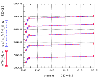
All the effects on the threshold voltage are based on the non-uniformity along the channel length. Regarding the channel width, the depletion region is always larger due to the existence of fringing fields at the side of the channel. This effect becomes very substantial as the channel width decreases and the depletion region underneath the fringing field becomes comparable to the depletion layer formed from the vertical field. This additional depletion region results in an increase of the threshold voltage with smaller channel widths, which is expressed by ΔVth(5).
Figure 75 Influence of Narrow Channel Effects on the Threshold Voltage
Threshold Voltage Reduction Through DIBL
The effect of the drain induced barrier lowering (DIBL) will be explained later. BSIM3 uses the following equation to model the DIBL effect in the threshold voltage:
Carrier Mobility Reduction
BSIM3v3 provides 3 different equations for the modeling of the mobility reduction. They can be selected by the flag MOBMOD.
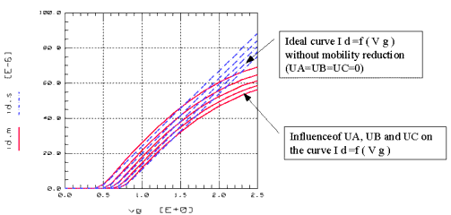
The influence of the mobility reduction parameters is demonstrated in the following figure where the simulated drain current with and without mobility reduction is shown.
Figure 76 Influence of Mobility Reduction
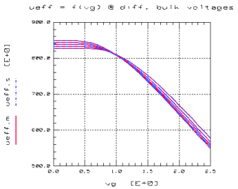
The following figure shows the effective mobility as a function of gate voltage and bulk-source voltage.
Figure 77 Effective Mobilityµeff as a Function of Gate- and Bulk-Source-Voltage
Effective Channel Length and Width
Effective Channel Length
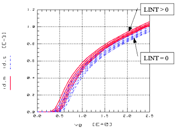
Figure 78 Influence of Channel Length Reduction on the Drain Current
The effective channel length is defined in BSIM3 as follows:
The channel length reduction on one side of the channel consists of several empirical terms as shown below:
The use of the model parameters LL, LLN, LWN, LW and LWL is very critical because they are only used for fitting purposes. On the other hand, they may be needed to achieve a good fit over a large area of channel lengths especially for processes with a minimum designed gate length of less than 0.25µm. The previous figure shows the influence of the geometrical channel length reduction LINT on the drain current of a short channel transistor while The following figure represents the channel length reduction according to Equation 67.
Figure 79 Channel Length Reduction dL as a Function of Channel Length L
Effective Channel Width
The effective channel width is defined in BSIM3 as follows:
The channel width reduction on one side of the channel consists of several empirical terms as shown below:
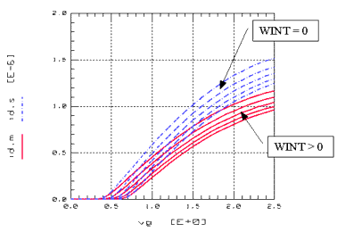
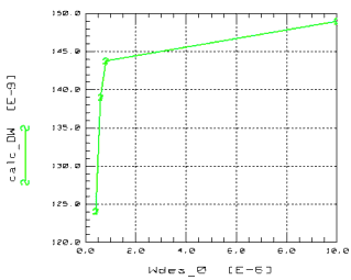
The use of the model parameters WL, WLN, WWN, WW, and WWL is very critical because they are only used for fitting purposes. On the other hand, they may be needed to achieve a good fit over a large area of channel widths especially for processes with a minimum designed gate width of less than 0.25µm. The following figure shows the influence of the geometrical channel width reduction WINT on the drain current of a narrow channel transistor while Figure 81 represents the channel width reduction according to Equation 69.
Figure 80 Influence of Channel Width Reduction on the Drain Current
Figure 81 Channel Width Reduction dW as a Function of Channel Width W
Drain Current
Single Equation for Drain Current
In contrast to former implementations of the BSIM3 model, the drain current is represented through a single equation in all three areas of operation (subthreshold region, linear region, and saturation region). Due to this single formula, all first order derivatives of the drain current are continuous, which is an important prerequisite for analog simulations.
In the case that no parasitic drain/source resistance is given, the equation for the drain current is given below:
This equation is valid for all three regions of operation of the MOS transistor because the voltages at drain, gate and bulk are replaced by effective drain voltage Vdseff, the effective gate voltage Vgsteff and the effective bulk voltage Vbseff, which are all defined by the continuous equations below:
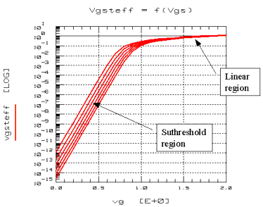
Equation 71 shows the effective (Vgs - Vth) voltage, where the factor n is defined in Equation 75.
Figure 82 Effective Voltage Vgs - Vth
The figure above shows Vgsteff in logarithmic scale. Vgsteff fits a linear function for values of Vgs greater than Vth while the subthreshold area is covered by the fit of an exponential function. Through this equation the first derivative is continuous between both operational regions (subthreshold and linear) of the MOS transistor.
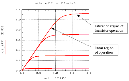
Equation 72 shows the effective drain source voltage, Vdseff:
The following figure shows Vdseff in both the linear and the saturation region of operation of the MOS transistor. Vdseff models the transition between linear and saturation region without discontinuity in the first derivative of the drain current.
Figure 83 Effective Voltage Vdseff
Drain Saturation Voltage Vdsat
The equation for the drain saturation voltage is divided into two cases, the intrinsic case with Rds = 0 and the extrinsic case with Rds > 0:
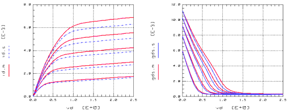
The influence of the maximum carrier velocity VSAT on the drain current Ids and the conductance gds is demonstrated in the following figure.
Figure 84 Influence of VSAT on Drain Current Ids and Conductance gds
Bulk Charge Effect
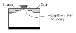
When the drain voltage is high, combined with a long channel length, the depletion depth of the channel is not uniform along the channel length. This will cause the threshold voltage to vary along the channel length and is called bulk charge effect. The following figure shows the depletion depth as a function of channel length. For long channels, this effect causes a reduction of the drain current.
Figure 85 Depletion Width along the Channel Length
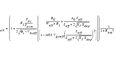
The bulk charge effect Abulk is modeled in BSIM3 with the parameters A0, AGS, B0, B1, and KETA as shown in Equation 74.
The influence on the drain current is shown in the following figure.
Figure 86 Influence of A0 and KETA on Ids at High Drain Voltages
Drain Current in the Subthreshold Region
The drain current in the subthreshold region is modeled in BSIM3v3 by the effective voltage Vgsteff. The model parameters VOFF and NFACTOR describe the subthreshold current for a large transistor, while the parameters CDSC, CDSCD, and CDSCB are responsible for modeling the subthreshold behavior as a function of channel length. All these parameters contribute to the factor n in the formula for Vgsteff (see Equation 71).
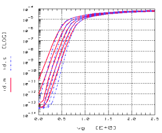
The influence of VOFF and NFACTOR on the drain current in the subthreshold region is shown in the following figure.
Figure 87 Influence of VOFF and NFACTOR on Drain Current in the Subthreshold Region
Parasitic Resistance
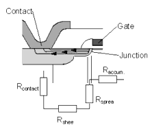
As MOS devices are scaled into the deep submicron region, both the conductance gm and the current of the device increase. Therefore the voltage drop across the source and drain series resistance becomes a non-negligible fraction of the applied drain source voltage. The resistance components associated with a MOSFET structure are shown in the following figure. These include the contact resistance (Rcontact) between metallization and source/drain area, the diffusion sheet resistance (Rsheet) of the drain/source area, the spreading resistance (Rspread) that arises from the current spreading from the channel, and the accumulation layer resistance (Raccum.).
Figure 88 Resistance Components of a MOS Device
These components are put together to form the following equation in the BSIM3v3:
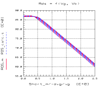
The diagram in the following figure visualizes the equation of Rds. It should be noted that BSIM3 assumes that the drain resistance is equal to the source resistance. This symmetrical approach may cause difficulties if a device with a nonsymmetrical drain source resistance, for example a DMOS power transistor, should be modeled. In this case, a scalable SPICE macro model should add the required behavior to BSIM3.
Figure 89 Drain Source Resistance Rds as a Function of Vg and Vb
With this enhancement, Equation 70 for the drain current can be rewritten:
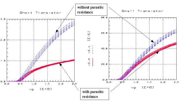
The influence of the parasitic resistance on the drain current is demonstrated for a SHORT and a SMALL transistor in the following figure.
Figure 90 Influence of Drain Source Resistance on Drain Current
Output Resistance
a) Early Voltage
The drain current in the saturation region of submicron MOSFETs is influenced by the effects of channel length modulation (CLM), drain induced barrier lowering (DIBL), and substrate current induced body effect (SCBE). These effects can be seen clearly looking at the output resistance Rout of the device, which is defined as:
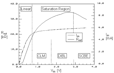
In the following figure, the measured drain current and the output resistance of an n-type MOS transistor with a channel length of 0.5 µm are shown.
Figure 91 Drain Current and Output Resistance in Linear and Saturation Region
The left most region in the figure above is the linear region, in which carrier velocity is not saturated. The output resistance is small because the drain current has a strong dependence on the drain voltage. The other three regions belong to the saturation region. The three physical effects CLM, DIBL, and SCBE can be seen in the saturation region and are discussed in the following sections.
With the output resistance, the equation for the drain current (Equation 78) is enhanced by two additional terms and can be rewritten as:
The behavior of the output resistance is modeled in BSIM3 in the same way as the Early voltage of a bipolar transistor is modeled in the Gummel-Poon model. The Early voltage is divided in two parts, VA due to DIBL and CLM and VASCBE due to SCBE. VA is given by:
where VAsat is the Early voltage at Vdsat:
b) Channel length modulation (CLM)
When the drain bias approaches the drain saturation voltage, a region of high electric field forms near the drain and the electron velocity in this region saturates. In saturation, the length ΔL of the high-field region increases by an expansion in the direction of the source with increasing drain-source voltage Vds and the MOSFET behaves as if the effective channel length has been reduced by ΔL. This phenomena is termed channel length modulation (CLM). CLM is not a special short-channel phenomenon, since the effect is present if a MOSFET is short or long. However, its relative importance increases and the effect on the saturated output conductance becomes distinctly more pronounced at shorter gate lengths.
The part of the Early voltage due to CLM is given by:
Figure 92 Channel Length Modulation (CLM)
c) Drain Induced Barrier Lowering (DIBL)
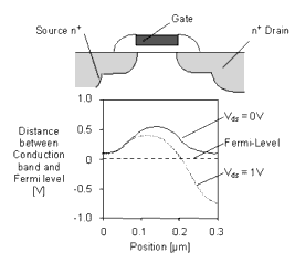
The depletion charges near source and drain are under the shared control of these contacts and the gate. In a short-channel device, this shared charge will constitute a relatively large fraction of the total gate depletion charge and can be shown to give rise to an increasingly large shift in the threshold voltage Vth with decreasing channel length L. Also, the shared depletion charge near drain expands with increasing drain-source bias, resulting in an additional Vds dependent shift in Vth. This effect is related to a drain voltage induced lowering of the injection barrier between the source and the channel and is termed the drain induced barrier lowering (DIBL). The following figure shows the band diagram at the semiconductor-insulator interface of an 0.1  m n-channel MOSFET simulated by a device simulator. The symmetrical profiles correspond to Vds = 0 and the asymmetrical profiles to Vds > 0. In the figure, the simulated potential barrier near the source is observed to decrease with increasing drain bias, which indicates the origin of the DIBL effect.
Figure 93 Band Diagram at Si-SiO2 Interface of a 0.1 µm MOSFET
The DIBL effect is modeled in BSIM3v3 with the following equations:
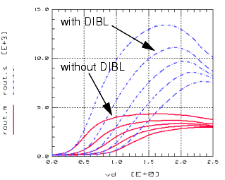
The following figure shows the influence of the DIBL effect on the output resistance of a short channel transistor.
Figure 94 Influence of Drain Induced Barrier Lowering (DIBL) effect on output resistance
d) Substrate Current Induced Body Effect (SCBE)
Substrate current is induced through hot electrons at high drain voltages, as described in Substrate Current. It is suggested that the substrate current increases exponentially with the applied drain voltage. The total drain current will change, because it is the sum of the channel current from the source as well as the substrate current. It can be expressed as:
The increase of the total drain current through hot electrons will be described by the part VASCBE of the Early voltage which results in a lowering of the output resistance for high drain voltage (following figure).
Figure 95 Substrate Current Body Effect (SCBE)
Substrate Current
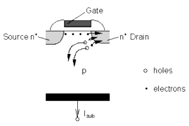
In a n-channel MOSFET, electrons in the channel experience a very large field near the drain. In this high field, some electrons coming from the source will be energetic enough to cause impact ionization, and additional electrons and holes are generated by avalanche multiplication. The high energy electrons are referred as hot electrons. The generated electrons are attracted to the drain, adding to the channel current, while holes are collected by the substrate contact, resulting in a substrate current, which is shown in the following figure.
Figure 96 Generation of Substrate Current in an n-channel MOSFET
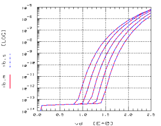
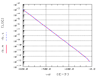
Figure 97 Substrate Current Ibs parameterized by Vg
The substrate current is described in BSIM3 by the following equation:
Drain/Bulk and Source/Bulk Diodes
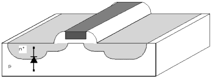
The following figure shows a pn-junction diode between the bulk and the drain of an n-type MOS Transistor.
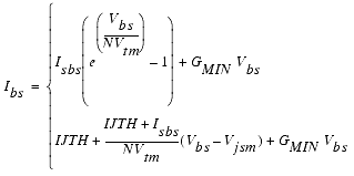
The drain/bulk and the source/bulk pn-junctions can be used as diodes in CMOS designs. BSIM3v3 offers a simple DC model for the current Ibs or Ibd flowing through these diodes.
where NJ is the emission coefficient of the source junction and the saturation current Isbs is calculated as:
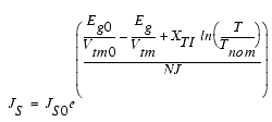
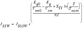
where JS is the saturation current density of the source/bulk diode, AS is the area of the source junction, JSSW is the sidewall saturation current density of the source/bulk diode, and PS is the perimeter of the source junction. JS and JSSW are functions of the temperature and can be described as:
- JS0 is the saturation current density (default is 10-4 A/m2)
- JS0SW is the sidewall saturation current density (default is 0)
- NVtm = NJ · (KbT/q)
- Vjsm = NVtm ln (ijth/Isbs + 1)
- JS0SW is the sidewall saturation current density (default is 0)
The current Ibs through the diode is shown in the following figure:
Figure 99 Current Ibs Through Diode
Consistency Check of DC measurement data for multiple measured devices
You can perform a quick consistency check of the measured data versus gate length, gate width, and temperature. If there are measurement errors, they can be easily identified using this additional check of DC measurement data.
Drain Saturation Current Idsat
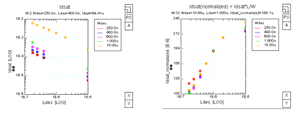
Displaying the absolute values of IDSAT versus the gate length of all measured devices does not easily show measurement errors because the absolute currents spread all over the diagram, as shown in the left part of the following figure.
In this diagram, absolute values of IDSAT versus L and W are displayed. IDSAT is determined at max. Vg, max. Vd, and Vb=0 for one temperature. Each dot represents one transistor and each color a different value of the transistors gate width W. The legend is shown to the right of the plot. If you select one of the dots, at the top of the plot the details of this specific transistor are shown. In our example of Idsat, the red dot in the middle of the plot is a transistor with W=250nm and L=400nm. The actual drain current of this geometry is also shown!
Figure 100 Left part: IDSAT = f(W, L); right part: IDSATnorm = f(W, L)
But if the same values (measured at the same temperature) are displayed in a normalized representation IDSATnorm = Idsat*L/W (see right part of the figure above), the values appear in a sorted way. They are shown from the transistors having the highest gate width values on top of the lower gate width transistors. The transistors having the smallest gate width values are shown at the lowest display position in the diagram.
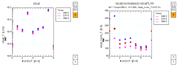
If the temperature measurements of the transistors are normalized as well, the measured data is again sorted. The following diagram shows IDSAT and IDSATnorm for devices with temperature measurements. Each color represents one temperature and each value of the x-axis represents one device.
Left part: IDSAT = f(temp, device); right part: IDSATnorm = f(temp, device)
Threshold voltage
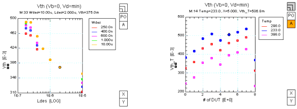
Similar normalized data representations are available for the threshold voltage Vth of measured devices, see the following figure. Vth is determined for each device at Vb=0 and low Vd. The following diagram shows Vth as a function of L, W (left part), and temperature (right part) for those devices. Vth is determined using the reference current method:



 1
1
