Each component
described in Section 4
can be decomposed into several first or second order
RC circuits.
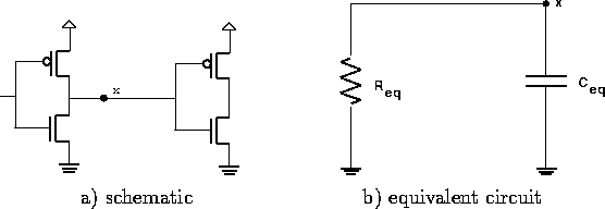
Figure 9-a shows a typical first-order circuit.
The time for node x to rise or fall can be determined using
the equivalent circuit of
Figure 9-b. Here, the pull-down path (assuming a
rising input) of the first stage is replaced by a resistance, and
the gate capacitances of the second stage and the drain
capacitance of the first stage are replaced by a single capacitor.
The resistances and capacitances
are calculated as shown in Sections 5.1
to 5.3. In stages in which the two gates are
separated by a long wire, parasitic capacitances and resistances
of the wire are included in ![]() and
and ![]() .
.
Figure 9: Example Stage
The delay of the circuit in Figure 9 can be estimated using an equation due to Horowitz [4] (assuming a rising input):
![]()
where ![]() is the switching voltage of the inverter,
is the switching voltage of the inverter,
![]() is the input rise time,
is the input rise time,
![]() is the output time constant assuming a step input (
is the output time constant assuming a step input ( ![]() ),
and b
is the fraction of the input swing
in which the output changes
(we used b=0.5). For a falling input with a fall time of
),
and b
is the fraction of the input swing
in which the output changes
(we used b=0.5). For a falling input with a fall time of ![]() ,
the above equation becomes:
,
the above equation becomes:
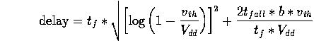
In this case, we used b=0.4.
The delay of a gate is defined as the time between the input
reaching the switching voltage (threshold voltage)
of the gate, and the output reaching the threshold voltage of
the following gate. If the gate drives a second gate with a different
switching voltage, the above equations need to be modified slightly.
If the switching voltage of the switching gate is ![]() and
the switching voltage of the following gate is
and
the switching voltage of the following gate is ![]() , then:
, then:
![]()
for a rising input, and

for a falling input.
As described in Section 4.2, the size of the wordline driver depends on the number of cells being driven. For a given array width, the capacitance driven by the wordline driver can be estimated by summing the gate capacitance of each pass transistor being driven by the wordline, as well as the metal capacitance of the line. Using this, and the desired rise time, the required pull-up resistance of the driver can be estimated by:
(recall that the desired rise time is assumed to be the time until the wordline reaches 50% of its maximum value).
Once ![]() is found, the required transistor width can be found using
the equation in Section 5.1.
Since this ``backwards analysis'' did not take into account the non-zero
input fall time, we then use
is found, the required transistor width can be found using
the equation in Section 5.1.
Since this ``backwards analysis'' did not take into account the non-zero
input fall time, we then use ![]() and
the wordline capacitance and calculate the adjusted
delay using Horowitz's equations as described earlier.
These transistor widths are also used to estimate the delay of the
final gate in the decoder.
and
the wordline capacitance and calculate the adjusted
delay using Horowitz's equations as described earlier.
These transistor widths are also used to estimate the delay of the
final gate in the decoder.