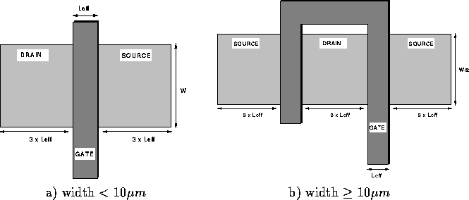
Figure 7 shows typical transistor
layouts for small and large transistors. We have assumed that
if the transistor width is larger than ![]() , the transistor is split as
shown in Figure 7-b.
, the transistor is split as
shown in Figure 7-b.
Figure 7: Transistor Geometries
The drain capacitance is composed of
both an area and perimeter component. Using the geometries in
Figure 7,
the drain capacitance for a single transistor can be obtained.
If the width is less than ![]() ,
,
![]()
where ![]() ,
, ![]() , and
, and ![]() are process dependent
parameters (there are two values for each of these: one for NMOS and one
for PMOS transistors).
are process dependent
parameters (there are two values for each of these: one for NMOS and one
for PMOS transistors). ![]() is the sum of the junction
capacitance due to the diffusion and the oxide capacitance due to the
gate/source or gate/drain overlap.
is the sum of the junction
capacitance due to the diffusion and the oxide capacitance due to the
gate/source or gate/drain overlap.
If the width is larger than ![]() , we assume the transistor is folded
(see Figure 7-b), reducing the drain capacitance to:
, we assume the transistor is folded
(see Figure 7-b), reducing the drain capacitance to:
![]()
Now, consider two transistors (with widths less than ![]() ) connected in
series, with only a single
) connected in
series, with only a single ![]() wide region acting as both
the source of the first transistor and the drain of the second.
If the first transistor is on, and the second transistor is off, the
capacitance seen looking into the drain of the first is:
wide region acting as both
the source of the first transistor and the drain of the second.
If the first transistor is on, and the second transistor is off, the
capacitance seen looking into the drain of the first is:
![]()
Figure 8 shows the situation if the transistors are wider
than ![]() . In this case, the capacitance seen looking into the drain of
the inner transistor (x in the diagram) assuming it is on but the outer
transistor is off is:
. In this case, the capacitance seen looking into the drain of
the inner transistor (x in the diagram) assuming it is on but the outer
transistor is off is:
![]()
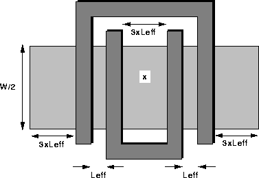
Figure 8: Two stacked transistors if each width ![]()
![]()