All but two of the stages along the cache's critical path can be approximated by simple first-order stages as in the previous section. The bitline and comparator equivalent circuits, however, require more complex solutions. Figure 10 shows an equivalent circuit that can be used for the bitline and comparator circuits. From [5], the delay of this circuit can be written as:
![]()
where ![]() is the voltage at the beginning of the transistion, and
is the voltage at the beginning of the transistion, and
![]() is the voltage at which the stage is considered to have
``switched'' (
is the voltage at which the stage is considered to have
``switched'' ( ![]() ). For the comparator,
). For the comparator, ![]() is
is ![]() and
and
![]() is the threshold voltage of the multiplexor driver.
For the bitline subcircuit,
is the threshold voltage of the multiplexor driver.
For the bitline subcircuit, ![]() is the precharged voltage of
the bitlines (
is the precharged voltage of
the bitlines ( ![]() ), and
), and ![]() is the voltage which causes the sense
amplifier output to fully switch (
is the voltage which causes the sense
amplifier output to fully switch ( ![]() ).
).
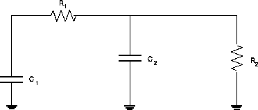
Figure 10: Equivalent circuit for bitline and comparator
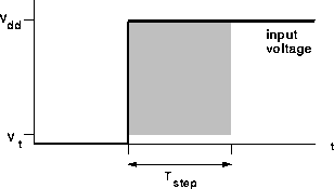
When estimating the bitline delay, a non-zero wordline rise time is taken
into account as follows. Figure 11 shows the wordline voltage
as a function of time for a step input. The time difference ![]() shown on the graph is the time after the input rises
(assuming a step input) until the output reaches
shown on the graph is the time after the input rises
(assuming a step input) until the output reaches ![]() (the output voltage is not shown on the graph).
An equation for
(the output voltage is not shown on the graph).
An equation for ![]() is given above. During this time,
we can consider the bitline being ``driven'' low.
Because the current sourced by the
access transistor can be approximated as
is given above. During this time,
we can consider the bitline being ``driven'' low.
Because the current sourced by the
access transistor can be approximated as
![]()
the shaded area in the graph can be thought of as the amount of
charge discharged before the output reaches
![]() .
This area can be calculated as:
.
This area can be calculated as:
![]()
( ![]() is the voltage at which the NMOS transistor begins to conduct).
is the voltage at which the NMOS transistor begins to conduct).
If we assume that the same amount of ``drive'' is required to drive
the output to ![]() regardless of the shape
of the input waveform, then we can calculate the output delay
for an arbitrary input waveform.
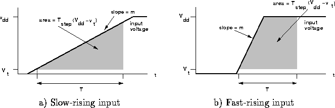
Consider Figure 12-a.
If we assume the area is the same as in Figure 11,
then we can calculate the value of T (delay adjusted for input rise time).
Using simple algebra, it is easy to show that
regardless of the shape
of the input waveform, then we can calculate the output delay
for an arbitrary input waveform.
Consider Figure 12-a.
If we assume the area is the same as in Figure 11,
then we can calculate the value of T (delay adjusted for input rise time).
Using simple algebra, it is easy to show that
![]()
where m is the slope of the input waveform (this can be estimated using
the delay of the previous stage). Note that the bitline delay is measured
from the time the wordline reaches ![]() . Unlike the version of the model
described in [3], the wordline rise time in this model is
defined as the time until the bitlines begin to discharge; this happens when
the wordline reaches
. Unlike the version of the model
described in [3], the wordline rise time in this model is
defined as the time until the bitlines begin to discharge; this happens when
the wordline reaches ![]() .
.
Figure 12: Non-zero input rise time
If the wordline rises quickly, as shown in Figure 12-b, then the algebra is slightly different. In this case,
![]()
The cross-over point between the two cases for T occurs when:
![]()
The non-zero input rise time of the comparator can be taken into account
similarly. The delay of the comparator is composed of two parts: the delay
of the timing chain and the delay discharging the output (see
Figure 5). The delay of the first three inverters in the
timing chain can be approximated using simple first-order RC stages as
described in Section 5.5. The time to discharge the
comparator output through the final inverter can be estimated using the
equivalent circuit of Figure 10 and taking into account the
non-zero input rise time using the same technique that was used for the
bitline subcircuit. In this case, the ``input'' is the output of the third
inverter in the timing chain (we assume the timing chain is long enough that
the ![]() and
and ![]() lines are stable). The discharging delay of the
comparator output is measured from the time the input reaches the threshold
voltage of the final timing chain inverter. The equations for this case can
be found in [3].
lines are stable). The discharging delay of the
comparator output is measured from the time the input reaches the threshold
voltage of the final timing chain inverter. The equations for this case can
be found in [3].