High Frequency Behavior
Macro Model for High Frequency Application
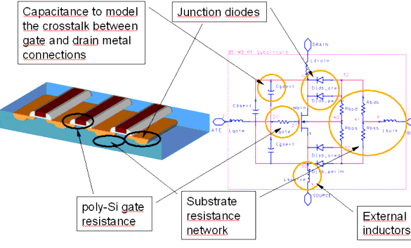
Using the BSIM3v3 model for the simulation of high frequency applications requires a major change in the model structure. A new concept of a SPICE simulation model for deep submicron devices based on the standard BSIM3v3.3.0 model was found, which is able to satisfy a correct DC simulation and the representation of the RF behavior of the MOS devices. The following figure shows the subcircuit used for RF simulation using the BSIM3 model together with an explanation of the physical structure responsible for each element of the subcircuit.
Figure 114 Equivalent Circuit for the SPICE Macro Model
|
|
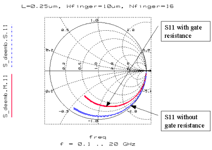
The model itself is implemented as the macro model shown above—no changes are done in the BSIM3v3.3.0 model code itself. This is the ultimate precondition for its use in a commercial circuit simulator that includes the BSIM3v3.3.0 model and makes it available to circuit design engineers. The BSIM3v3.3.0 model already consists of a non-quasi-static model and an accurate capacitance model, which makes it the ideal base for RF simulations. However, the description of the resistance behavior of a transistor is very poor. In the BSIM3v3.3.0 model itself, no gate resistance is included. Due to the nature of the MOS transistor, such a resistance cannot be seen in the DC operation region. However, looking at the real existing poly silicon gates of modern MOS devices, there is a resistance which cannot be neglected in AC simulations. This resistance, Rgate, has a major influence on the reflection coefficient S11 of an input signal to the MOS transistor as demonstrated in the following figure.
It should be noted that the parameter Rgate in this high frequency model is used to fit the input reflection of the MOS transistor. Therefore, it is very likely that Rgate has a different value as the measured sheet resistance of the poly-Si gate during process characterization on PCMs using for instance a van-der-Pauw test structure.
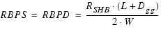
The second enhancement in the RF BSIM3v3.3.0 macro model is a resistance network for the substrate resistance, which is described by four resistors RBPD, RBPS, RBDB, and RBSB [7, 8]. The substrate resistance can be seen in the reverse-reflection coefficient S22 at the output of the transistor. Together with the resistance network, the internal drain-bulk and source-bulk junction diodes of the BSIM3v3.3.0 model are replaced by the external elements Djdb_area, Djdb_perim, Djsb_area, and Djsb_perim. The decoupling diodes account for the same voltage dependant values of the bottom and the sidewall capacity as the internal junction capacitances. This replacement is the prerequisite for a correct modeling of the substrate resistance.
With this approach, the model is valid for both the DC and the RF behavior of the transistor.
Figure 115 Influence of gate resistance on input reflection S11
|
|
Single Subcircuit Model for BSIM3v3 RF Transistors
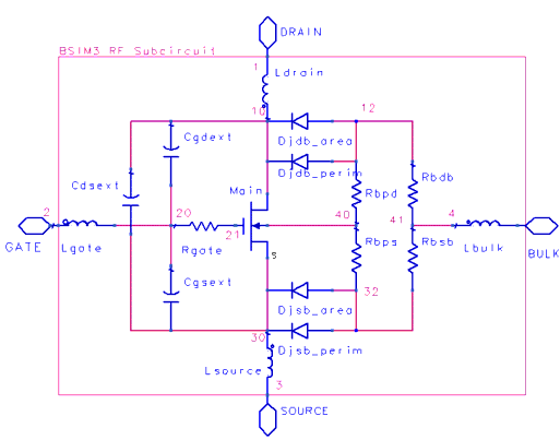
The macro model approach results in a subcircuit for single RF MOS transistors, which the following circuit file shows (according to Figure 114).
Figure 116 Subcircuit for RF modeling of single transistors using the BSIM3-model
|
|
Following is part of the SPICE netlist used for single transistors in BSIM3v3 RF modeling.
 LINK CIRC Circuit
 {
 data
 {
 circuitdeck
 {
  .OPTIONS GMIN=1.0E-14
  * -----------------------------------------------------------------------------
  * Single subcircuit model for BSIM3v3.3.0 RF n-type devices
  *
  * Simulator: UCB Spice3e2
  * Model: BSIM3 Modeling Package
  * Date: 25.04.2003
  * Origin: ICCAP_ROOT/..../bsim3/code/circuits/spice3/cir/rf_nmos_single.cir
  * -----------------------------------------------------------------------------
  *
  .subckt bsim3_rf_extract 1 2 3 4
  *
  *--- BSIM3 model card ---------------------------------------------------------
 #echo .MODEL BSIM3_HF NMOS
 #echo + LEVEL=$mpar(LEVEL=8) VERSION=3.2.4 BINUNIT=$mpar(BINUNIT=2)
 #echo + MOBMOD=$mpar(MOBMOD=1 CAPMOD=$mpar(CAPMOD=3) NOIMOD=$mpar(NOIMOD=1)
 #echo + PARAMCHK=$mpar(PARAMCHK=1)
 #echo + DELTA=$mpar(DELTA=0.01)TNOM=$mpar(TNOM=27)TOX=$mpar(TOX=7.5E-9)
 #echo + TOXM=$mpar(TOXM=7.5E-9)
 #echo + NCH =$mpar(NCH=1.7e17) XJ=$mpar(XJ=1.5E-7) NGATE=$mpar(NGATE=0) RSH =$mpar(RSH=0)
 #echo + VTH0=$mpar(VTH0=0.7) K1=$mpar(K1=0.53) K2=$mpar(K2=-0.013) K3=$mpar(K3=0)
 #echo + K3B =$mpar(K3B=0) W0=$mpar(W0=2.5E-6) NLX =$mpar(NLX=0.174u) DVT0=$mpar(DVT0=2.2)
 #echo + DVT1=$mpar(DVT1=0.53) DVT2=$mpar(DVT2=-0.032) DVT0W=$mpar(DVT0W=0)
 #echo + DVT1W=$mpar(DVT1W=5.3E6)
 #echo + DVT2W=$mpar(DVT2W=-0.032) ETA0=$mpar(ETA0=0) ETAB=$mpar(ETAB=0)
 #echo + DSUB=$mpar(DSUB=0.56)
 #echo + U0=$mpar(U0=670) UA=$mpar(UA=2.25E-9) UB=$mpar(UB=5.87E-19) UC=$mpar(UC=4.65E-11)
 #echo + VSAT=$mpar(VSAT=8e4) A0=$mpar(A0=1) AGS =$mpar(AGS=0) B0=$mpar(B0=0)
 #echo + B1=$mpar(B1=0) KETA=$mpar(KETA=-0.047) A1=$mpar(A1=0) A2=$mpar(A2=1)
 #echo + RDSW=$mpar(RDSW=0) PRWB=$mpar(PRWB=0) PRWG=$mpar(PRWG=0) WR=$mpar(WR=1)
 #echo + WINT=$mpar(WINT=0) WL=$mpar(WL=0) WLN =$mpar(WLN=1) WW=$mpar(WW=0)
 #echo + WWN =$mpar(WWN=1) WWL =$mpar(WWL=0) DWG =$mpar(DWG=0) DWB =$mpar(DWB=0)
 #echo + LINT=$mpar(LINT=0) LL=$mpar(LL=0) LLN =$mpar(LLN=1) LW=$mpar(LW=0)
 #echo + LWN =$mpar(LWN=1) LWL =$mpar(LWL=0)
 #echo + VOFF=$mpar(VOFF=-0.08) NFACTOR=$mpar(NFACTOR=1) CIT =$mpar(CIT=0)
 #echo + CDSC=$mpar(CDSC=2.4E-4)
 #echo + CDSCB=$mpar(CDSCB=0) CDSCD=$mpar(CDSCD=0) PCLM=$mpar(PCLM=1.3)
 #echo + PDIBLC1=$mpar(PDIBLC1=0.39)
 #echo + PDIBLC2=$mpar(PDIBLC2=0.0086) PDIBLCB=$mpar(PDIBLCB=0.0) DROUT=$mpar(DROUT=0.56)
 #echo + PSCBE1=$mpar(PSCBE1=4.24E8)
 #echo + PSCBE2=$mpar(PSCBE2=1.0E-5) PVAG=$mpar(PVAG=0) VBM =$mpar(VBM=-3)
 #echo + ALPHA0=$mpar(ALPHA0=0) ALPHA1=$mpar(ALPHA1=0) BETA0=$mpar(BETA0=30)
 #echo + JS=1e-20 JSW =1.0E-20 NJ=1 IJTH=$mpar(IJTH=0.1)
 #echo + CJ=0 MJ=0.5 PB=1 CJSW=0
 #echo + MJSW=0.33 PBSW=1 CJSWG=$mpar(CJSWG=5E-10) MJSWG=$mpar(MJSWG=0.33)
 #echo + PBSWG=$mpar(PBSWG=1) CGDO=$mpar(CGDO=0) CGSO=$mpar(CGSO=0)
 #echo +CGBO=$mpar(CGBO=0)
|
 #echo +CGBO=$mpar(CGBO=0) CGSL=$mpar(CGSL=0) CGDL=$mpar(CGDL=0)
 #echo + CKAPPA=$mpar(CKAPPA=0.6) CF=$mpar(CF=0)
 #echo + NOFF=$mpar(NOFF=1) VOFFCV=$mpar(VOFFCV=0) ACDE=$mpar(ACDE=1)
 #echo + MOIN=$mpar(MOIN=15) DLC=$mpar(DLC=0) DWC=$mpar(DWC=0)
 #echo + LLC=$mpar(LLC=0) LWC=$mpar(LWC=0) LWLC=$mpar(LWLC=0)
 #echo + WLC=$mpar(WLC=0) WWC=$mpar(WWC=0) WWLC=$mpar(WWLC=0)
 #echo + CLC=$mpar(CLC=0.1E-6) CLE=$mpar(CLE=0.6) ELM=$mpar(ELM=2)
 #echo + XPART=$mpar(XPART=0.5) KT1=$mpar(KT1=-0.11) KT1L=$mpar(KT1L=0)
 #echo + KT2=$mpar(KT2=0.022) UTE=$mpar(UTE=-1.5) UA1=$mpar(UA1=4.31E-9)
 #echo + UB1=$mpar(UB1=-7.6E-18) UC1=$mpar(UC1=-5.6E-11) AT=$mpar(AT=3.3E4)
 #echo + PRT=$mpar(PRT=0) XTI=$mpar(XTI=3.0) TPB=$mpar(TPB=0)
 #echo + TPBSW=$mpar(TPBSW=0) TPBSWG=$mpar(TPBSWG=0)
 #echo + TCJ=$mpar(TCJ=0) TCJSW=$mpar(TCJSW=0) TCJSWG=$mpar(TCJSWG=0)
 #echo + AF=$mpar(AF=1.5) EF=$mpar(EF=1.5) KF=$mpar(KF=1e-17) EM=$mpar(EM=4.1E7)
 #echo + NOIA=$mpar(NOIA=2e29) NOIB=$mpar(NOIB=5e4) NOIC=$mpar(NOIC=-1.4e-12)
 *--- Parasitic diode model cards ----------------------------------------------
 #echo .MODEL bsim_diode_area D
 #echo + CJO=$mpar(CJ=5E-4) VJ=$mpar(PB=1) M=$mpar(MJ=0.5)
 #echo + IS=$mpar(JS=1.0E-4) N=$mpar(NJ=1)
 #echo .MODEL bsim_diode_perim D CJO=$mpar(CJSW=5E-10) VJ=$mpar(PBSW=1)
 #echo + M=$mpar(MJSW=0.33) IS=$mpar(JSW=1.0E-12) N=$dpar(CALC.NJSW=1)
 * --------- Gate network ------------------------------------------------------
 CGDEXT 20 10 0.1f
 CGSEXT 20 30 0.1f
 RGATE 20 21 100
 LGATE 2 20 1p
 * --------- Drain network -----------------------------------------------------
 CDSEXT 10 30 0.1f
 LDRAIN 1 10 1p
 * --------- Source network ----------------------------------------------------
 LSOURCE 3 30 1p
 * --------- Substrate network -------------------------------------------------
 * Diodes are for n-type MOS transistors
 #echo Djdb_area 12 10 bsim_diode_area AREA=$dpar(x_rf_transistor.AD=10e-12)
 #echo Djdb_perim 12 10 bsim_diode_perim AREA=$dpar(x_rf_transistor.PD=22e-6)
 #echo Djsb_area 32 30 bsim_diode_area AREA=$dpar(x_rf_transistor.AS=10e-12)
 #echo Djsb_perim 32 30 bsim_diode_perim AREA=$dpar(x_rf_transistor.PS=22e-6)
 RBDB 12 40 100
 RBSB 32 40 100
 RBPD 12 41 100
 RBPS 32 41 100
 LBULK 4 40 1p
 *--- call single MOSFET -------------------------------------------------------
 #echo MAIN 10 21 30 41 BSIM3_HF
 #echo + L=$dpar(x_rf_transistor.L=1u) W=$dpar(x_rf_transistor.W=10e-6)
 #echo + AD=$dpar(x_rf_transistor.AD=10e-12) AS=$dpar(x_rf_transistor.AS=10e-12)
 #echo + PD=$dpar(x_rf_transistor.PD=22e-6) PS=$dpar(x_rf_transistor.PS=22e-6)
 #echo + NRS=$dpar(x_rf_transistor.NRS=0) NRD=$dpar(x_rf_transistor.NRD=0)
 #echo + NQSMOD=$mpar(NQSMOD=0)
 .ends
 }
 }
 }
|
The single BSIM3 RF model represents exactly one measured test device, the substrate resistance network uses fixed values for the resistors RBPS, RBPD, RBDB, and RBSB. Also, the external parasitics (L, C, ...) are fixed and valid only for one measured device. Using this approach, the parameters extracted are valid only for a specific transistor geometry, which means you must have RF parameters for each of your possible device geometries. This requires measurement and library creation for every transistor geometry in your design.
Design engineers often need to have scalable transistors for easy design processes. Therefore, extensions are made to use a scalable BSIM3 model. Those are described in the following section.
Fully Scalable Subcircuit Model for BSIM3v3 RF Transistors
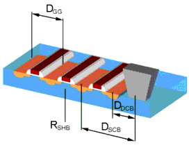
The following figure shows a cross section of a multifinger RF MOSFET with the distances marked from the bulk connection point to the physical transistor connections.
Figure 117 Distances between the bulk connection and the terminals of a multifinger RF transistor
|
|
The distances are:
| • |
DDCB: distance between bulk connection point and drain |
| • |
DDCS: distance between bulk connection point and source |
| • |
DGG: distance between gate stripes |
Additionally, the sheet resistance of the bulk connection, RSHB, is needed.
Implementations according to "MOS Transistor Modeling for RF IC Design" [8] and our own findings to model a scalable substrate resistance behavior are leading to the following equations, which are implemented into the SPICE subcircuit for the fully scalable BSIM3 RF model.
Using the distances according to the previous figure, the resistors are calculated from:
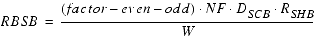
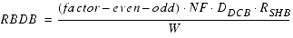
factor-even-odd = 0.5 for even number of fingers (NF)
factor-even-odd = 1 for odd number of fingers (NF)
The values of the elements of the SPICE equivalent circuit are calculated from device dimensions of the actual device (W, L, NF...) and additional model parameters like the gate sheet resistance RSHG.
Following is a SPICE netlist for the fully scalable BSIM3 model.
 LINK CIRC Circuit
 {
 data
 {
 circuitdeck
 {
 *
 * ------------------------------------------------------------------------------------
 * Fully scalable subcircuit model for BSIM3v3 RF n-type devices
 * Simulator: UCB Spice3e2
 * Model: BSIM3 Modeling Package
 * Date: 08.11.2003
 * Origin: ICCAP_ROOT/..../bsim3/circuits/spice3/cir/rf_nmos_scale.cir
 * ------------------------------------------------------------------------------------
 *
 .subckt bsim3_rf_extract 1 2 3 4
 *
 *--- Information for model implementation --------------------------------------------
 *
 * Due to the limitation of UCB spice3e2, the equations for the scaled RF model behavior are
included in the DUT parameters of the DUT RF_Transistor_Scale in the IC-CAP model
BSIM3_RF_Extract
 *
 * To implement this scalable model in your target simulator, please include those equations
using the appropriate syntax in the final model deck.
 *
 *--- BSIM3 model card ----------------------------------------------------------------
 #echo .MODEL BSIM3_HF NMOS
 #echo + LEVEL=$mpar(LEVEL=8) VERSION=3.2.4 BINUNIT=$mpar(BINUNIT=2)
 #echo + MOBMOD=$mpar(MOBMOD=1) CAPMOD=$mpar(CAPMOD=3) NOIMOD=$mpar(NOIMOD=1)
 #echo + PARAMCHK= $mpar(PARAMCHK=1) DELTA=$mpar(DELTA=0.01) TNOM=$mpar(TNOM=27)
 #echo + TOX=$mpar(TOX=7.5E-9) TOXM=$mpar(TOXM=7.5E-9)
 #echo + NCH=$mpar(NCH=1.7e17) XJ=$mpar(XJ=1.5E-7) NGATE=$mpar(NGATE=0) RSH=$mpar(RSH=0)
 #echo +
 #echo + VTH0=$mpar(VTH0=0.7) K1=$mpar(K1=0.53) K2=$mpar(K2=-0.013) K3=$mpar(K3=0)
 #echo + K3B=$mpar(K3B=0) W0=$mpar(W0=2.5E-6) NLX=$mpar(NLX=0.174u) DVT0=$mpar(DVT0=2.2)
 #echo + DVT1=$mpar(DVT1=0.53) DVT2=$mpar(DVT2=-0.032) DVT0W=$mpar(DVT0W=0)
 #echo + DVT1W=$mpar(DVT1W=5.3E6) DVT2W=$mpar(DVT2W=-0.032)
 #echo + ETA0=$mpar(ETA0=0) ETAB=$mpar(ETAB=0) DSUB=$mpar(DSUB=0.56)
 #echo +
 #echo + U0=$mpar(U0=670) UA=$mpar(UA=2.25E-9) UB=$mpar(UB=5.87E-19) UC=$mpar(UC=4.65E-11)
 #echo + VSAT=$mpar(VSAT=8e4) A0=$mpar(A0=1) AGS=$mpar(AGS=0) B0=$mpar(B0=0)
 #echo + B1=$mpar(B1=0) KETA=$mpar(KETA=-0.047) A1=$mpar(A1=0) A2=$mpar(A2=1)
 #echo + RDSW=$mpar(RDSW=0) PRWB=$mpar(PRWB=0) PRWG=$mpar(PRWG=0) WR=$mpar(WR=1)
 #echo +
 #echo + WINT=$mpar(WINT=0) WL=$mpar(WL=0) WLN=$mpar(WLN=1) WW=$mpar(WW=0)
 #echo + WWN=$mpar(WWN=1) WWL=$mpar(WWL=0) DWG=$mpar(DWG=0) DWB=$mpar(DWB=0)
 #echo + LINT=$mpar(LINT=0) LL=$mpar(LL=0) LLN=$mpar(LLN=1) LW=$mpar(LW=0)
 #echo + LWN=$mpar(LWN=1) LWL=$mpar(LWL=0)
 #echo + VOFF=$mpar(VOFF=-0.08) NFACTOR=$mpar(NFACTOR=1) CIT=$mpar(CIT=0)
 #echo + CDSC=$mpar(CDSC=2.4E-4)
 #echo + CDSCB=$mpar(CDSCB=0) CDSCD=$mpar(CDSCD=0) PCLM=$mpar(PCLM=1.3)
 #echo +PDIBLC1=$mpar(PDIBLC1=0.39)
|
 #echo + PDIBLC2=$mpar(PDIBLC2=0.0086) PDIBLCB=$mpar(PDIBLCB=0.0) DROUT=$mpar(DROUT=0.56)
 #echo + PSCBE1=$mpar(PSCBE1=4.24E8)
 #echo + PSCBE2=$mpar(PSCBE2=1.0E-5) PVAG=$mpar(PVAG=0) VBM=$mpar(VBM=-3)
 #echo + ALPHA0=$mpar(ALPHA0=0) ALPHA1=$mpar(ALPHA1=0) BETA0=$mpar(BETA0=30)
 #echo +
 #echo + JS=1e-20 JSW=1.0E-20 NJ=1 IJTH=$mpar(IJTH=0.1)
 #echo +
 #echo + CJ=0 MJ=0.5 PB=1 CJSW=0
 #echo + MJSW=0.33 PBSW=1 CJSWG=$mpar(CJSWG=5E-10) MJSWG=$mpar(MJSWG=0.33)
 #echo + PBSWG=$mpar(PBSWG=1) CGDO=$mpar(CGDO=0) CGSO=$mpar(CGSO=0) CGBO=$mpar(CGBO=0)
 #echo + CGSL=$mpar(CGSL=0) CGDL=$mpar(CGDL=0) CKAPPA=$mpar(CKAPPA=0.6) CF=$mpar(CF=0)
 #echo + NOFF=$mpar(NOFF=1) VOFFCV=$mpar(VOFFCV=0) ACDE=$mpar(ACDE=1) MOIN=$mpar(MOIN=15)
 #echo + DLC=$mpar(DLC=0) DWC=$mpar(DWC=0) LLC=$mpar(LLC=0) LWC=$mpar(LWC=0)
 #echo + LWLC=$mpar(LWLC=0) WLC=$mpar(WLC=0) WWC=$mpar(WWC=0) WWLC=$mpar(WWLC=0)
 #echo + CLC=$mpar(CLC=0.1E-6) CLE=$mpar(CLE=0.6)
 #echo + ELM=$mpar(ELM=2) XPART=$mpar(XPART=0.5)
 #echo +
 #echo + KT1=$mpar(KT1=-0.11) KT1L=$mpar(KT1L=0) KT2=$mpar(KT2=0.022) UTE=$mpar(UTE=-1.5)
 #echo + UA1=$mpar(UA1=4.31E-9) UB1=$mpar(UB1=-7.6E-18) UC1=$mpar(UC1=-5.6E-11)
 #echo + AT=$mpar(AT=3.3E4)
 #echo + PRT=$mpar(PRT=0) XTI=$mpar(XTI=3.0) TPB=$mpar(TPB=0) TPBSW=$mpar(TPBSW=0)
 #echo + TPBSWG=$mpar(TPBSWG=0) TCJ=$mpar(TCJ=0) TCJSW=$mpar(TCJSW=0) TCJSWG=$mpar(TCJSWG=0)
 #echo +
 #echo + AF=$mpar(AF=1.5) EF=$mpar(EF=1.5) KF=$mpar(KF=1e-17) EM=$mpar(EM=4.1E7)
 #echo + NOIA=$mpar(NOIA=2e29) NOIB=$mpar(NOIB=5e4) NOIC=$mpar(NOIC=-1.4e-12)
 *
 *
 *--- Parasitic diode model cards ----------------------------------------------------
 #echo .MODEL bsim_diode_area D
 #echo + CJO=$mpar(CJ=5E-4) VJ=$mpar(PB=1) M=$mpar(MJ=0.5)
 #echo + IS=$mpar(JS=1.0E-4) N=$mpar(NJ=1)
 *
 #echo .MODEL bsim_diode_perim D
 #echo + CJO=$mpar(CJSW=5E-10) VJ=$mpar(PBSW=1) M=$mpar(MJSW=0.33)
 #echo + IS=$mpar(JSW=1.0E-12) N=$dpar(CALC.NJSW=1)
 *
 *
 *--- Additional model parameters necessary for scalability---------------------------
 * - scalable external capacitors and inductors to account for cross coupling in the metal
stripes and additional delay due to large sizes
 * - a scalable substrate network
 * - a scalable channel length reduction
 *
 #echo * CGDEXT0=$mpar(CGDEXT0=1e-9) ext. cap. gate-drain per gate width and finger [F/m]
 #echo * CGSEXT0=$mpar(CGSEXT0=1e-9) ext. cap. gate-source per gate width and finger [F/m]
 #echo * CDSEXT0=$mpar(CDSEXT0=1e-9) ext. cap. drain-source per gate width and finger [F/m]
 #echo * RSHG=$mpar(RSHG=25) gate sheet resistance [Ohm sq]
 #echo * LDRAIN0=$mpar(LDRAIN0=1e-6) drain inductance per gate width and gate finger [H/m]
 #echo * LGATE0=$mpar(LGATE0=1e-6) gate inductance per gate width and gate finger [H/m]
|
 #echo * LSOURCE0=$mpar(LSOURCE0=1e-6) source inductance per gate width and finger [H/m]
 #echo * LBULK0=$mpar(LBULK0=1e-6) bulk inductance per gate width and finger [H/m]
 #echo * RSHB=$mpar(RSHB=25) bulk sheet resistance [Ohm sq]
 #echo * DSBC=$mpar(DSBC=2e-6) distance source implant to bulk contact [m]
 #echo * DDBC=$mpar(DDBC=2e-6) distance drain implant to bulk contact [m]
 #echo * DGG=$mpar(DGG=2e-6) distance gate to gate [m]
 #echo * DL0=$mpar(DL0=0) basic channel length reduction correction [m]
 #echo * DL1=$mpar(DL1=0) channel length reduction correction 1. and 2. outer fingers [m]
 #echo * DL2=$mpar(DL2=0) channel length reduction correction outer fingers [m]
 *
 *
 * --------- Gate network ------------------------------------------------------------
 #echo LGATE 2 20 $dpar(CALC.LGATE=0.1p)
 #echo RGATE 20 21 $dpar(CALC.RGATE=10)
 #echo CGDEXT 20 10 $dpar(CALC.CGDEXT=0.1f)
 #echo CGSEXT 20 30 $dpar(CALC.CGSEXT=0.1f)
 *
 * --------- Drain network -----------------------------------------------------------
 #echo LDRAIN 1 10 $dpar(CALC.LDRAIN=0.1p)
 #echo CDSEXT 10 30 $dpar(CALC.CDSEXT=0.1f)

 * --------- Source network ----------------------------------------------------------
 #echo LSOURCE 3 30 $dpar(CALC.LSOURCE=0.1p)
 *
 * --------- Substrate network -------------------------------------------------------
 * Diodes are for n-type MOS transistors
 *
 #echo Djdb_area 12 10 bsim_diode_area AREA=$dpar(x_rf_transistor.AD=10e-12)
 #echo Djdb_perim 12 10 bsim_diode_perim AREA=$dpar(x_rf_transistor.PD=22e-6)
 *
 #echo Djsb_area 32 30 bsim_diode_area AREA=$dpar(x_rf_transistor.AS=10e-12)
 #echo Djsb_perim 32 30 bsim_diode_perim AREA=$dpar(x_rf_transistor.PS=22e-6)
 *
 #echo RBDB 12 40 $dpar(CALC.RBDB=100)
 #echo RBSB 32 40 $dpar(CALC.RBSB=100)
 #echo RBPD 12 41 $dpar(CALC.RBPD=100)
 #echo RBPS 32 41 $dpar(CALC.RBPS=100)
 *
 #echo LBULK 4 40 $dpar(CALC.LBULK=0.1p)
 *
 *--- call single MOSFET -----------------------------------------------------------
 #echo MAIN 10 21 30 41 BSIM3_HF
 #echo + L=$dpar(x_rf_transistor.L=1u) W=$dpar(x_rf_transistor.W=10e-6)
 #echo + AD=$dpar(x_rf_transistor.AD=10e-12) AS=$dpar(x_rf_transistor.AS=10e-12)
 #echo + PD=$dpar(x_rf_transistor.PD=22e-6) PS=$dpar(x_rf_transistor.PS=22e-6)
 #echo + NRS=$dpar(x_rf_transistor.NRS=0) NRD=$dpar(x_rf_transistor.NRD=0)
 #echo + NQSMOD=$mpar(NQSMOD=0)
 *
 .ends
 }
 }
 }
|
Modeling Strategy
Modeling the AC behavior of a MOS device with the BSIM3v3 model heavily depends on the accurate modeling of the DC curves and the capacitances at low frequencies, for example, 10kHz to 1MHz. However, more and more applications, especially in the telecommunication industry, require the modeling of MOS transistors for the use in a frequency range of 1 to 10 GHz. Therefore, S-parameter measurements have to be done (see also Test Structures for S-parameter Measurements) to cover this frequency range by a proper device model.
As is pointed out, using the BSIM3v3 model for high frequency applications requires some special attention to the modeling strategy. We found the following procedure to give the most accurate results:
| • |
Measurement of DC and CV curves. |
| • |
Extraction of the BSIM3v3 model parameters from DC and CV measurements with a special emphasis on a physically based extraction strategy. Here, model parameters should not be used for fitting purposes, they should have a correct physical meaning. |
| • |
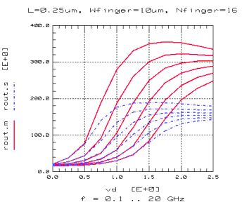
The modeling of the output characteristic Id=f(Vds) and the output resistance Rout=f(Vds) is very important for further S-parameter measurements (see Figure 121 and Figure 120). |
| • |
Performing S-parameter measurements and proper de-embedding of parasitics. |
| • |
The starting points of the S-parameter curves at the lowest frequency can be modeled by fitting the curves with DC and capacitance parameters. The following diagrams describe this influence on the high frequency behavior. |
Figure 118 Incorrectly Modeled Drain Current
|

|
Figure 119 Incorrectly Modeled Output Characteristic
|
|
Figure 120 Influence of Incorrectly Modeled Output Characteristic on S21
|
|
| • |
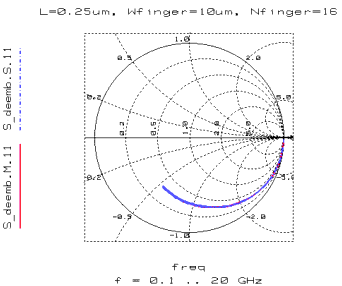
Extraction of the gate resistance from the input reflection S11 (see the following figure) |
| • |
Verification of the gate-drain overlap capacitance for higher frequencies |
| • |
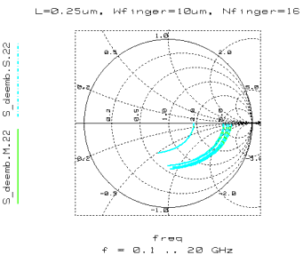
Extraction of the substrate resistance network parameters from S22 (see the following figure) |
| • |
If a good fitting could not be found, additional peripheral elements like inductances at drain, gate, or source should be added in a further sub-circuit |
Figure 121 Input Reflection Parameter S11
|
|
Figure 122 Output Reflection Parameter S22
|
|
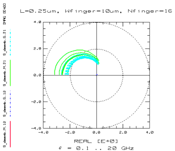
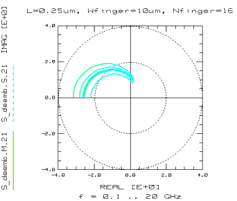
Figure 123 Forward Transmission Parameter S21
|
|
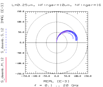
Figure 124 Reverse Transmission Parameter S12
|
|
|