Print version of this Book (PDF file)
Capacitance Model
Please use the model bsim3_tutor_cv.mdl provided with the BSIM3v3 Modeling Package to visualize the capacitance model parameters. Load the file into IC-CAP and run the different macros to see how certain parameters affect the device behavior of a deep submicron MOS transistor.
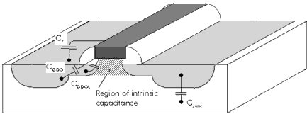
The capacitance in a MOS transistor can be divided into three different parts:
| • | Junction capacitance CJunc between source/drain and the bulk region |
| • | Capacitance of the extrinsic MOS transistor which consists of: |
| • | The outer fringing capacitance CF between polysilicon gate and the source/drain |
| • | The overlap capacitance CGDO between the gate and the heavily doped source/drain regions |
| • | The overlap capacitance CGDOL between the gate and the lightly doped source/drain regions |
| • | Capacitance of the intrinsic MOS transistor in the region between the metallurgical source and drain junction when the gate is at flat band voltage. |
These different parts of the capacitance of a MOS transistors are shown in the following figure. The following three sections explain each type of capacitance and its implementation in the BSIM3v3 model.
Figure 102 Different Parts of the Capacitance of a MOS Transistor
Junction Capacitance
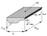
The source/drain-bulk junction capacitance can be divided into three components as shown in the following figure. The calculation is shown for the drain-bulk junction capacitance. The source-bulk capacitance is calculated in the same way with the same model parameters.
The overall junction capacitance Cjdb is given by:
- CAREA is the bottom area capacitance
- CSW is the sidewall or peripheral capacitance along the three sides of the junction's field oxide
- CSWG is the sidewall or peripheral capacitance along the gate oxide side of the junction
- CSW is the sidewall or peripheral capacitance along the three sides of the junction's field oxide
Figure 103 Dimensions of Drain/Source Region and Different Capacitance Parts
- AD area of bottom side of pn junction, given as SPICE model parameter
- Cjbd capacitance per unit area of the drain-bulk junction
- Cjbd capacitance per unit area of the drain-bulk junction
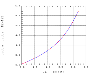
Cjbd is calculated according to the following equation and is shown in the following figure.
Figure 104 Bottom Area Capacitance Cjbd as a Function of Vg
Peripheral sidewall capacitance CSW along the field oxide
PD
total perimeter of pn junction, given as SPICE model parameter
Weff
effective gate width of transistor, calculated in SPICE
Cjbdsw
capacitance per unit length
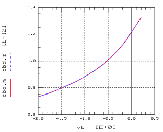
Cjbdsw is calculated according to the following equation and is shown in the following figure:
Figure 105 Sidewall Capacitance Cjbdsw as a Function of Vg
Peripheral sidewall capacitance CSWG along the gate oxide
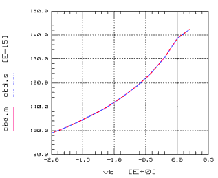
Cjbdswg is calculated according to the following equation and is shown in the following figure.
Figure 106 Sidewall Capacitance Cjbdswg Along the Gate Oxide as a Function of Vg
Extrinsic Capacitance
As mentioned in the introduction to this chapter, the extrinsic capacitance of a MOS transistor consists of the following three components:
| • | the outer fringing capacitance CF between polysilicon gate and the source/drain |
| • | the overlap capacitance CGDO between the gate and the heavily doped source/drain regions |
| • | the overlap capacitance CGDOL between the gate and the lightly doped source/drain regions |
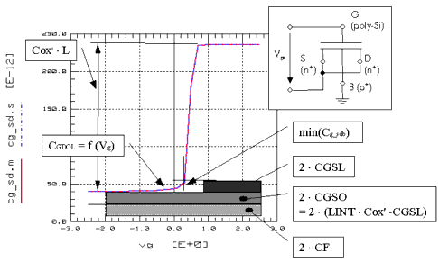
The contribution of these different components to the overall extrinsic capacitance is demonstrated in the following figure and Figure 108.
Figure 107 Different Components of the Extrinsic Capacitance
Figure 108 Overlap Capacitance Between Gate and Drain/Source/Bulk
a) Fringing Capacitance
The fringing capacitance of a MOS transistor consists of a bias independent outer fringing capacitance and a bias dependent inner fringing capacitance. In the present release of the BSIM3v3 model, only the bias independent outer fringing capacitance is implemented. Experimentally, it is virtually impossible to separate this capacitance with the overlap capacitance. Nonetheless if the model parameter CF is not given, the outer fringing capacitance can be calculated with the following equation:
b) Overlap Capacitance
In BSIM3v3 an accurate model for the overlap capacitance is implemented. In old capacitance models this capacitance is assumed to be bias independent. However, experimental data show that the overlap capacitance changes with gate to source and gate to drain biases. In a single drain structure or the heavily doped S/D to gate overlap region in a LDD structure, the bias dependence is the result of depleting the surface of the source and drain regions. Since the modulation is expected to be very small, this region can be modeled with a constant capacitance. However in LDD MOSFETs a substantial portion of the LDD region can be depleted, both in the vertical and lateral directions. This can lead to a large reduction of overlap capacitance. This LDD region can be in accumulation or depletion.
In BSIM3v3, a single equation is implemented for both regions by using such smoothing parameters as Vgsoverlap and Vgdoverlap for the source and drain side, respectively. Unlike the case with the intrinsic capacitance, the overlap capacitances are reciprocal. In other words, Cgsoverlap = Csgoverlap and Cgdoverlap = Cdgoverlap.
The model equations for the overlap capacitance are shown for the drain overlap capacitance and are identical for the source overlap capacitance:
Overlap charge per gate width:
for the measurement and simulation conditions given in Figure 107, this results in the overlap capacitance:
The model parameter CGDO in Equation 101 can be calculated by the following equation:
where DLC represents the channel length reduction in the BSIM3v3 capacitance model. Please see the next section for more details about DLC:
Intrinsic Capacitance
a) Geometry for Capacitance Model
The BSIM3v3 model uses different expressions for the effective channel length Leff and the effective channel width Weff for the I-V and the C-V parts of the model.
The geometry dependence for the intrinsic capacitance part is given as the following:
Lactive and Wactive are the effective length and width of the intrinsic device for capacitance calculations. The parameter ΔL is equal to the source/drain to gate overlap length plus the difference between drawn and actual poly gate length due to processing (gate printing, etching, and oxidation) on one side. The Lactive parameter extracted from the capacitance method is a close representation of the metallurgical junction length (physical length).
Figure 109 Dimensions of a MOSFET
While the authors of the BSIM3v3 model suggest to use a parameter LINT for the I-V model, which is different from DLC, other literature sources [3] propose that LINT should have the same value as DLC. This approach is also implemented in the BSIM3v3 Modeling Package to ensure that the extracted values of the channel length reduction are very close to the real device physics. Therefore, the channel length reduction LINT for the I-V model will be set to DLC from the C-V model extracted from capacitance measurements.
b) Intrinsic Capacitance Model
The intrinsic capacitance model that is implemented in the BSIM3 model is based on the principle of conservation of charge. There are a few major considerations in modeling the intrinsic capacitance of a deep submicron MOS transistor:
| • | The difficulty in capacitance measurement, especially in the deep submicron regime. At very short channel lengths, the MOSFET intrinsic capacitance is very small while the conductance is large. |
| • | Charge can only be measured at high impedance nodes (i.e., the gate and substrate nodes), only 8 of the 16 capacitance components in an intrinsic MOSFET can be directly measured. An alternative solution is to use a 2-D device simulator. |
| • | The access to the internal charges in a simulator. |
Therefore, this section presents no details about the intrinsic charge formulations. Please refer to the BSIM3v3 manual [1] for more information. Only the basic principles are described here.
To ensure charge conservation, terminal charges instead of the terminal voltages are used as state variables. The terminal charges Qg, Qb, Qs, and Qd are the charges associated with the gate, bulk, source, and drain. The gate charge is comprised of mirror charges from 3 components:
| • | The channel minority (inversion) charge (Qinv) |
| • | The channel majority (accumulation) charge (Qacc) |
| • | The substrate fixed charge (Qsub) |
The accumulation charge and the substrate charge are associated with the substrate node while the channel charge comes from the source and drain nodes:
The inversion charges are supplied from the source and drain electrodes. The ratio of Qd and Qs is the charge partitioning ratio. Existing charge partitioning schemes are 0/100, 50/50 and 40/60 (given by the model parameter XPART = 0, 0.5, and 1) which are the ratios of Qd to Qs in the saturation region.
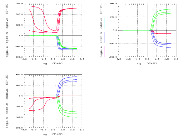
From these four terminal charges, 9 transcapacitances C(terminal,voltage) are calculated inside the BSIM3 model as partial derivatives with respect to the voltages Vgb, Vdb, and Vsb. The abbreviation can be interpreted as:
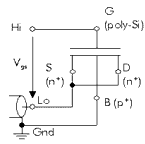
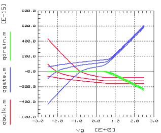
The 9 transcapacitances previously introduced are shown in the following three plots for a simulation setup as shown in the following figure:
Figure 110 Simulation and Measurement Setup for Overlap Capacitances
Figure 111 Terminal charges Qg, Qb and Qd
Figure 112 Partial derivatives of Qg, Qb and Qd with respect to Vdb, Vgb and Vsb
The Overall Capacitance in BSIM3
In previous sections, the three components of the BSIM3 capacitance model were introduced. Now when an AC simulation is performed the capacitance, which can be measured at the terminals, is composed of different parts of junction capacitances, extrinsic capacitances, and intrinsic capacitances.
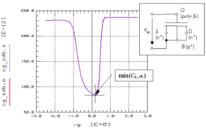
The following figure shows, as an example, the capacitance components for the overlap capacitance between gate and bulk/source/drain as simulated according to the following circuit description:
Figure 113 Different Parts of Overlap Capacitance C_Gate_SDB
The overlap capacitance C_Gate_SDB consists of:
Other capacitances can be calculated in the same way. Please refer to the BSIM3 manual for more details.


 0:
0:

