 Research
MEMS, with their multifunctionality and miniaturized forms, are increasingly making unique contributions to a variety of application fields. They however often encounter difficulties when interacting with external worlds due to material incompatibility. This is largely attributed to the fact that the range of materials available for conventional MEMS fabrication is significantly limited. There are a vast range of high-performance engineering materials as well as emerging nanomaterials that could be incorporated in MEMS to advance their capability. This research focuses on bridging the gap between diverse resource of non-traditional materials and MEMS towards creating new application opportunities.
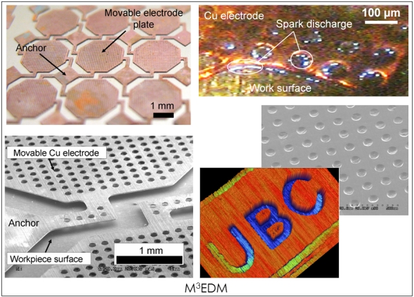
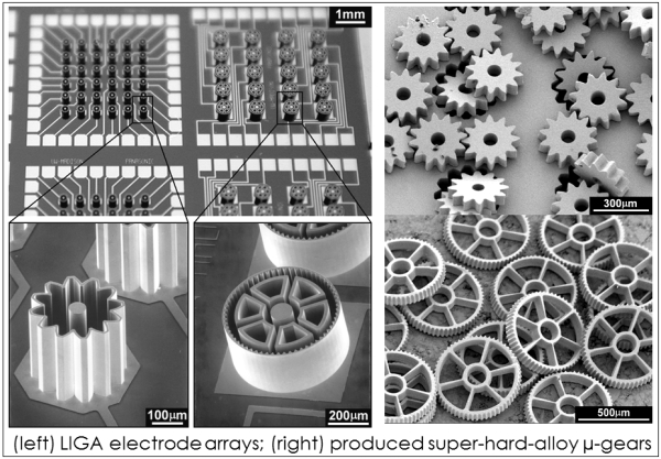
Micro-electro-discharge machining (µEDM) is a powerful and versatile micromachining technique as it can be applied to any type of electrical conductors. The process thermally etches a material using high-frequency pulses of micro arc discharge generated between the material and the tip of cylindrical microelectrode. We are investigating the physics of this discharge process and developing novel µEDM methods. One focus has been on converting the mode of the process from serial to parallel, by utilizing arrayed microelectrodes with distributed power control. To this end, we developed microelectrode arrays through lithographic processes and demonstrated batch-mode µEDM with high parallelness using the arrays, showing >100x throughput improvement compared with conventional µEDM methods. Along this line, we also demonstrated the first MEMS-based µEDM called M3EDM, in which arrays of electrostatic actuators were created on the sample surface to drive microelectrodes for µEDMing. This approach provides a unique solution to high-throughput micropatterning of extremely large-area samples.
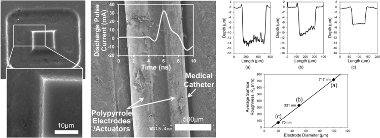
Polypyrrole and other conducting polymers are of interest in actuators, sensors, energy storage devices, and organic electronics. The patterning of these polymers in both macro and micro domains can be challenging, particularly polypyrrole due to its insolubility. We showed the first micropatterning of polypyrrole through a µEDM approach, by establishing high-frequency pulses of miniaturized electrical discharge on the polymer. Microstructures with surface roughness of 70 nm were produced with sub-micron depth control. The process was used for electrical partitioning of polypyrrole film deposited on a medical catheter, with a focus on the application to "smart" catheters that use patterned polypyrrole as integrated actuators.
This study involves the methods based on EDM as well as on mechanical manipulation of the nanotubes. Refer to the Carbon Nanotube Forest section for details.
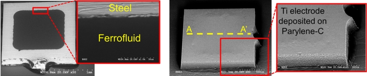
We have developed a non-lithographic method to create suspended movable diaphragms using the magnetic fluid called ferrofluid as a liquid-phase sacrificial layer in the microfabrication process. Parylene C is directly deposited on the ferrofluid sacrificial layer filled in a cavity in vacuum, forming a movable diaphragm suspended on the cavity after magnetically removing the fluid using a permanent magnet. This approach enables extremely simple, fast, and low-cost production of capacitive MEMS sensors while eliminating the need for photolithographic, bonding, thermal, or chemical process. We demonstrated a stainless-steel-based capacitive pressure sensor by leveraging this novel micromachining approach.
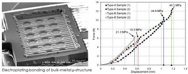
Hybrid MEMS enabled by integration of micromachined functional bulk materials is a promising path to achieving novel functionality and high performance in the devices. Assembly of such microstructures often involves various requirements including high bonding strength, electrical coupling, heat transfer, and compatibility with planar microfabrication processes and wafer-scale integration. We have developed an electroplating-based bonding technique that fulfills these key features, This room-temperature process enables assembly of bulk micromachined structures with microelectronic circuits and other heat sensitive components with high bonding strength and has been applied to the integration of shape-memory-alloy micro actuators with their driving circuits.
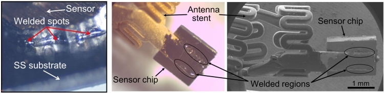
Another approach to hybrid MEMS integration being investigated is laser microwelding. This process has been shown to be very effective in bonding of stainless-steel-based MEMS chips on metallic substrates or devices. The microwelded bond was found to provide twice the mechanical strength and ~6x electrical conductance compared with a conductive epoxy case. Microwelding of the stainless-steel chip of capacitive pressure sensor was verified to preserve its sensing performance. We demonstrated sensor integration on stainless-steel antenna stents using this approach toward "smart" stent application.
Jump to other research theme:
The main page of Research