Print version of this Book (PDF file)
Simulation Input and Output Requirements
The following input and output requirements for each simulation type are also required for the corresponding measurement types.
DC Simulation
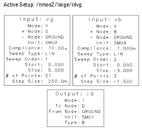
The following table describes the input and output specifications required for a valid setup for DC simulation and the following figure shows an example of input and output specifications for a MOSFET id versus vg setup.
V
LIN, LOG, LIST, SYNC, CON
V, I
I
LIN, LOG, LIST, SYNC, CON
V, I
Figure 13 Example Input and Output, DC Simulation
AC Simulation
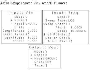
The following table describes the input and output specifications required for a valid setup for AC simulation. The following figure shows an example of input and output specifications for simulating the output voltage versus frequency of an inverting operational amplifier.
Figure 14 Example Input and Output, AC Simulation
Transient Simulation
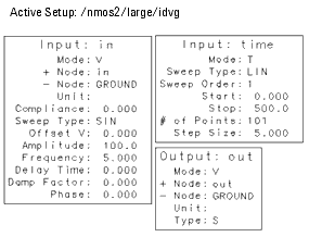
The following table describes the input and output specifications required for a valid setup for Transient simulation and the following figure shows an example of input and output specifications for voltage versus time characteristics of a differential pair.
Figure 15 Example Input and Output, Transient Simulation
Noise Simulation
The following tables describe the input and output specifications required for a valid setup for Noise simulation depending on the simulator being used.
CV Simulation
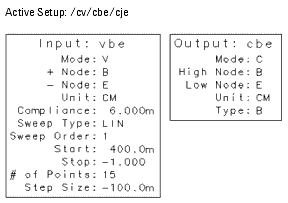
The following table describes the input and output specifications required for a valid setup for CV simulation and the following figure shows an example of input and output specifications for a BJT base-emitter pn-junction capacitance versus voltage setup.
The frequency at which the CV simulation is performed can be specified using the System Variable CV_FREQ in Hz. If this variable is not specified, the simulation will be performed at 1-MG (Hz).
Note
Figure 16 Example Input and Output, CV Simulation
2-Port Simulation
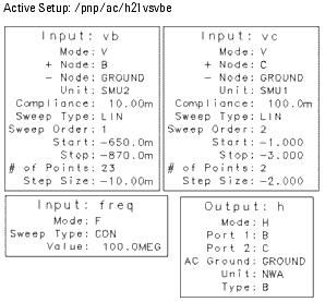
The following table describes the input and output specifications required for a valid setup for 2-port simulation and the following figure shows an example of input and output specifications for an H21-parameter versus Vbe setup.
F
LIN, LOG, LIST, CON
S, H, Y, Z, K, A, F
1. Exactly one frequency sweep required.
V
LIN, LOG, LIST, SYNC, CON
S, H, Y, Z, K, A, F
2. Exactly one 2-port output (S,H,Y,Z,K or A) required.
I
LIN, LOG, LIST, SYNC, CON
S, H, Y, Z, K, A, F
3. Only ADS supports F output.1
4. Exactly one 2-port output required for F output.
5. F output can be multiple outputs.
12-Port noise simulation supports ADS only. If the SIMULATOR is not equal to hpeesofsim, the following error message appears.
Error: in "Output xxxx"
High frequency noise output is not supported with current simulator.
Mode
High Frequency Noise
F
High frequency noise mode type
Data Type
Noise Figure
NF
Noise figure data
Yes1, 2
Gamma Opt
GAMMAOPT
Optimum source reflection coefficients
No
Equivalent R Noise
RN
Equivalent noise resistance data
No
Min Noise Figure
NFMIN
Minimum noise figure data
No
Equivalent Noise Temperature
TE
Equivalent Noise Temperature data
Yes *, †
1The port field of the NF/TE noise parameter can not be blank.
If the port field set NF/TE type is blank, the following error message appears.
Error: in "Output xxxx"
Blank output node name for NF specified.
2The port name of the NF/TE parameter must be consistent with the port name of the 2-port output.
The port name of the NF/TE output noise must be equal to one of the port names of the 2-port output; otherwise, the following error message appears.
Error: in "Output xxxx"
Port "xx" is not consistent with the 2-port specification node: "xx" or "xx"
Figure 17 Example Input and Output, 2-Port Simulation
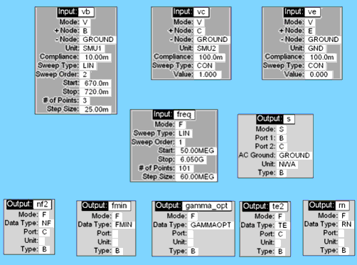
Active Setup: /bjt_ncehf/sp/sparm_noise_bias
Figure 18 Example Input and Output, 2-Port Noise Simulation
2-Port Circuits
An L-network of LCR is added to port 1 and port 2 to uncouple an AC signal from a DC bias to simulate a DUT using AC analysis. To see an actual input circuit deck, use the Simulator Debugger.
When the port 1 has an AC source, its signal goes through an R whose value is defined by TWOPORT_Z0 and its default is 50 [ohm]. Then this signal is given to a port 1 through a C whose value is defined by TWOPORT_C, and its default is 100 [F]. The port 1 is also connected to a DC bias source through an L whose value is defined by TWOPORT_L and its default is 100 [H]. The port 2 has a similar L-network whose AC source is replaced by a short to ground.
There are two circuits in a single deck to represent two cases where the port 1 has a source and the port 2 has a source. These circuits are generated and added to a DUT for simulators.
TDR Simulation
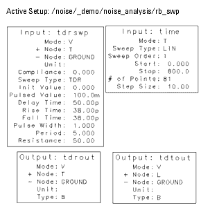
The following table describes the input and output specifications required for a valid setup for TDR (Time Domain Reflect) simulation. The following figure shows an example of input and output specifications for simulating the reflected and transmitted signal of a simple TDR circuit.
T
LIN, LIST, CON
V
1. Exactly one time sweep required.
V
LIN, LOG,L IST, SYNC, CON, TDR
V
2. Only voltage outputs allowed.
I
LIN, LOG, LIST, SYNC, CON
V
3. Exactly one voltage sweep of type TDR required.
Figure 19 Example of Input and Output Specifications for a TDR Simulation
Harmonic Balance Simulation
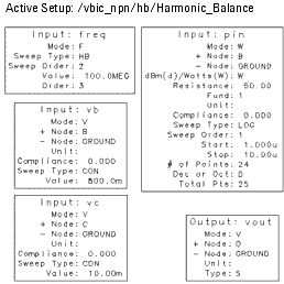
The following table describes the input and output specifications required for a valid setup for Harmonic Balance simulation and the following figure shows an example of input and output specifications for a BJT power-in versus power-out setup.
V
LIN, LOG, LIST, SYNC, CON, AC
V, I
1. Exactly one frequency sweep with Sweep Type = HB required.
I
LIN, LOG, LIST, SYNC, CON, AC
V, I
2. At least one AC source required: V or I (AC), or W.
F
HB
V, I
3. The Test Circuit includes elements such as DCFEED or DCBLOCK.
W (Power)
LIN, LOG, LIST, CON
V, I
4, Units for the Power (W) source can be set to dBm(d) or Watts (W).
Figure 20 Example of Input and Output Specifications for a Harmonic Balance Simulation