Print version of this Book (PDF file)
CV Modeling
Capacitance Model
To accurately model MOSFET behavior, a good capacitance model considering intrinsic and extrinsic (overlap/fringing) capacitances is important.
BSIM4 provides three options to select different capacitance models. These are the models from BSIM3v3.2, which are taken without changes. There is only one exception: Different parameters for source and drain sides are introduced, which are used to precisely model different doping concentrations and so on.
The model flag CAPMOD allows three values. CAPMOD = 0 uses piece-wise and simple equations, whereas with CAPMOD = 1 and 2 uses smooth and single equation models.
For CAPMOD = 0, VTH is taken from a long-channel device; for CAPMOD = 1 and 2, VTH is consistent with the BSIM4 DC model.
The overlap capacitance model uses a bias-independent part to model the effective overlap capacitance between gate and heavily doped source/drain regions and a gate-bias dependent part between the gate and the lightly doped source/drain regions.
Fringing capacitances between gate and source as well as gate and drain are modeled bias-independent.
Intrinsic Capacitance Modeling
All capacitances in Intrinsic Capacitance Model formulations are derived from terminal charges instead of terminal voltages to ensure charge conservation.
Long channel device models assume the mobility to be constant and no channel length modulation occurs. However, with shrinking device dimensions, velocity saturation and channel length modulation are to be considered to accurately model device behavior.
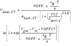
For capacitance modeling in BSIM4, a drain bias is defined, at which the channel charge becomes constant.
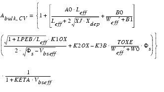
For capacitance modeling, Abulk is defined different from DC:
Numerical simulation has shown that the charged layer under the gate of a MOSFET has a significant thickness in all regions of operation. Therefore, a Charge-Thickness Model has been introduced in BSIM4. This model uses a capacity in series with the oxide capacitance Cox and an effective oxide capacitance is used:
DC charge layer thickness in accumulation and depletion is calculated by:
By introducing the VFB term in Equation 40, the calculation is valid for N+ or P+ poly-silicon gates and future gate materials too.
Using TEMPMOD=2, the calculation of Vfbzb becomes temperature dependent and is calculated the following way:
Intrinsic Capacitance Model Equations
There are three intrinsic capacitance models to choose from using the model flag CAPMOD. Additionally, there are three charge partitioning schemes: 40/60, 50/50, and 0/100. Those schemes describe distribution of the intrinsic capacitance charges between drain and source side.
The exact formulations for the different operation regimes and charge partitioning schemes are in the UC Berkeley manual [1] on pages 7-13 to 7-19.
Fringing Capacitance Models
The fringing capacitance consists of a bias-independent outer fringing capacitance and an inner fringing capacitance, bias-dependent. The outer fringing capacitance is modeled in BSIM4 (if not given) through:
The inner capacitance is not modeled.
Overlap Capacitance Model
For accurate simulation results, especially the drain side overlap capacitance has to be modeled exactly because the influence of this capacitance is amplified by the gain of the transistor (Miller effect). Formerly used capacitance models assume a bias -independent overlap capacitance. However, experimental data show a gate-bias dependent overlap capacitance, which is invoked using CAPMOD = 1 or 2. Using CAPMOD = 0, a simple bias-independent model is invoked.
For CAPMOD = 0, the overlap charges are expressed by:
Gate-to-source overlap charge:
The parameters CGSO and CGDO are calculated (if not given) by:
If
DLC is given and > 0
if CGSO < 0: CGSO = 0
if CGDO < 0: CGDO = 0
Else
If CGBO is not given, it is calculated by:
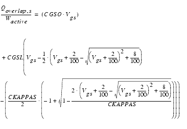
For CAPMOD = 1 or 2, the bias-dependent overlap charge is modeled at the source side by:
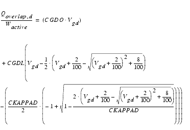
and the gate overlap charge by:


