Print version of this Book (PDF file)
Binning of Model Parameters
Usage of binned models in a simulator
The binning idea
The idea of binning is to provide different model parameter sets for a scalable model (e.g., a MOS device) according to the device dimensions. In the case of MOSFETs, the validity of such a parameter set is determined by LMIN, LMAX, WMIN, WMAX for each bin.
Major commercial simulators like HSPICE, Spectre, and ADS support the binning feature for semiconductor models. However, it is not included in standard UC Berkeley SPICE3f5!
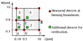
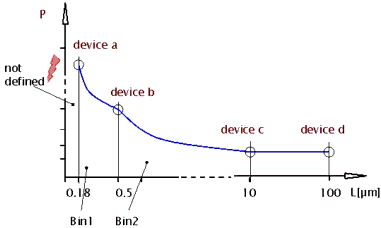
Figure 148 Binned model according to the measured devices
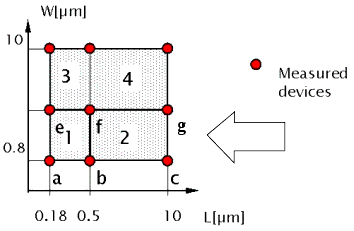
Lets take the example shown in the diagram above: we have 4 different bins with 4 different parameter sets. If we look only at the bins with the smallest width (see the arrow above), we still have 2 different parameter sets: set #1 and set #2.
The simulator would take the bins according to the following table:
L < LMIN(bin1)
Error: not specified!
LMIN(bin1)
 L < LMAX(bin1)
BIN1 interpolated
LMIN(bin2)
L < LMAX(bin2)BIN2 interpolated
L
 LMAX(bin2)
Error: not specified!
Please note: LMAX(bin1) = LMIN(bin2)
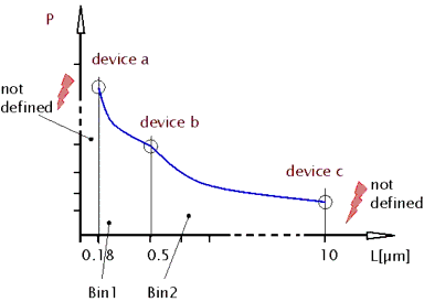
The simulator now calculates an effective model parameter P(L) from the different binned parameter sets and the actual gate length of the device to simulate.
In addition, inside a certain bin, the parameter itself is interpolated so that we end up with the following diagram:
Figure 149 Calculation of binned model parameters
Advanced binning approaches
As the diagram in the previous figure clearly shows, the model is defined only inside the gate length of the characterized devices. This is a critical condition, because the following two scenarios are very common for MOS devices:
| • | It is very usual to use a transistor with, for example, L = 10 µm as the largest measured device and to extrapolate the parameter set to devices with larger gate lengths. This is not a problem because the 10 um transistor already behaves like an ideal MOS transistor without short and narrow channel effects. |
| • | For statistical simulations, the gate length and widths are overlaid by a statistical variation to reflect variations in lithography. If gate length or gate width are already at the boundary of the available model bins, this would not work. |
Both described effects would cause no problem using the normal BSIM3 or BSIM4 model without binning. However, having the restrictions of the binning implementation in the simulators, the following two alternatives would help to overcome this bottleneck.
Extension of binning to include virtual devices
The first idea is to add additional model sets for areas in the L-W-space, which are not fully covered by measured devices. The following diagram shows such a scenario:
Figure 150 Extension of binning
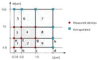
The binned model parameter sets for region 1 through 4 have been determined from measured devices. Now, for the generation of the parameter set of region 9, it is assumed that the parameters for device d are equal to the parameters of device c and parameters from h are equal the parameters from g. The gate length of d and h are selected so large, that they cover all useful applications. The diagram in the following figure shows the principal calculation of the parameter P over an available range of gate lengths L.
Figure 151 Calculation of binned model parameters with extensions
Extraction of binned model parameters
General algorithm
| • | For each device Di, at the boundary of the bins, the original parameter Poi = Pi is determined using a circuit/model parameter set without the binning feature! |
| • | For each bin, the parameter is interpolated for the actual length and width according to the following equation: |
| • | The binning parameters Pi, PLi, PWi, PPi for one bin must be determined from the original parameters Poi and Poi+1. This is also very important to make sure that the parameter P is continuous at the boundary between two bins. That's the reason why the devices at the edges of a bin are used to determine the parameters! |
Implementation into the BSIM3/4 Modeling Packages
Output for the selected simulator
The output of the BSIM3/BSIM4 Modeling Packages is ready for use with a simulator. One of the major problems is that the basic SPICE3F5 simulator of UC Berkeley does not include the binning features of ADS, HSPICE, or Spectre. Therefore, binning will be limited to those commercial simulators!
The following listing shows a typical binned library for ADS:
 ; example ADS BinModel
 ; Min[ , ] (inclusive)
 ; Max[ , ] (exclusive, inclusive if Max=Min)
 ;
 model my_nmos BinModel \
       Model[1]="my_nmos1" \
       Model[2]="my_nmos2" \
       Model[3]="my_nmos3" \
       Model[4]="my_nmos4" \
       Model[5]="my_nmos5" \
       Model[6]="my_nmos6" \
       Model[7]="my_nmos7" \
       Model[8]="my_nmos8" \
       Model[9]="my_nmos9" \
       Param[1]="Length" \
       Param[2]="Width" \
       Min[1,1]=L1 Max[1,1]=L2 Min[1,2]=W1 Max[1,2]=W2 \
       Min[2,1]=L2 Max[2,1]=L3 Min[2,2]=W1 Max[2,2]=W2 \
       Min[3,1]=L3 Max[3,1]=L4 Min[3,2]=W1 Max[3,2]=W2 \
       Min[4,1]=L1 Max[4,1]=L2 Min[4,2]=W2 Max[4,2]=W3 \
       Min[5,1]=L2 Max[5,1]=L3 Min[5,2]=W2 Max[4,2]=W3 \
       Min[6,1]=L3 Max[6,1]=L4 Min[6,2]=W2 Max[4,2]=W3 \
       Min[7,1]=L1 Max[7,1]=L2 Min[7,2]=W3 Max[4,2]=W4 \
       Min[8,1]=L2 Max[8,1]=L3 Min[8,2]=W3 Max[4,2]=W4 \
       Min[9,1]=L3 Max[9,1]=L4 Min[9,2]=W3 Max[4,2]=W4
 ;
 model my_nmos1 MOSFET NMOS=1 PMOS=0 etc ...
 model my_nmos2 MOSFET NMOS=1 PMOS=0 etc ...
 model my_nmos3 MOSFET NMOS=1 PMOS=0 etc ...
 model my_nmos4 MOSFET NMOS=1 PMOS=0 etc ...
 model my_nmos5 MOSFET NMOS=1 PMOS=0 etc ...
 model my_nmos6 MOSFET NMOS=1 PMOS=0 etc ...
 model my_nmos7 MOSFET NMOS=1 PMOS=0 etc ...
 model my_nmos8 MOSFET NMOS=1 PMOS=0 etc ...
 model my_nmos9 MOSFET NMOS=1 PMOS=0 etc ...
Definition of binning areas
One of the major disadvantages of the binning approach is, that the scalability feature of a model is not fully taken into account. With the binning approach, all binned parameters are interpolated using the same functions 1/L and 1/W.
Typically a scalable model behavior, for example, the threshold voltage, is replaced by the binning approach. The following example will make this more clear:
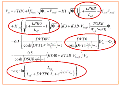
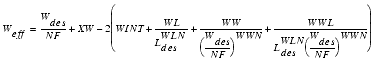
The threshold voltage of BSIM4 is given above. It is a complex equation that describes length and width related effects. In a binned model, parameters describing those effects (DVT0, DVT1, LPE0, e.t.c.) are normally not used. Instead the basic threshold voltage parameters VTH0, K1, and K2 together with the binning extensions PVTH0, LVTH0, WVTH0, ...., WK2 are describing these effects.
If we have a Vth-function like in the following figure, it is clear that a proper selection of binning areas is necessary to cover this behavior!
Figure 152 Typical Vth behavior of a 0.18um CMOS process (n-type)
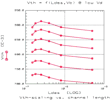
Figure 153 Two different binning scenarios
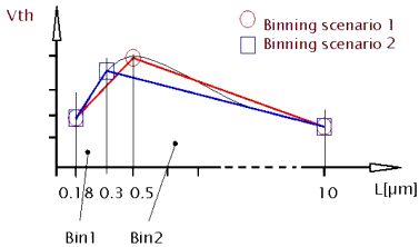
The previous diagram clearly shows the difficulty in defining proper boundaries for the different binning areas. While the binning scenario 1 covers the typical behavior of Vth, the second scenario would miss the point of maximum Vth.
To verify the correct behavior, additional devices between the binning boundaries are necessary, especially in the critical areas with minimum gate lengths and widths as outlined below: