Structure of the BSIM4 RF Simulation Model
The BSIM4 model consists of some major features that make it ideal for use in real high frequency simulations. It contains:
| • |
scalable gate resistance |
| • |
dedicated thermal noise model formulation |
| • |
different device layouts (multifinger devices) are taken into account |
| • |
substrate resistance network with correct connection to the main transistor through parasitic diodes |
| • |
New in BSIM4.3.0: Horseshoe substrate contacts |
While the first three effects are fully scalable, which means the influence of the device dimensions like gate length or width is already included in the model formulation, the substrate resistance effect included into BSIM4 has not included any of this information up to version 4.3.0. To specify the substrate resistance effect, only fixed values for up to 5 different resistors could have been set. However, in reality, the substrate resistance effect depends on sheet resistance of the body, number of gate fingers and width of the devices.
Due to this shortcoming, it is not possible to generate one fully scalable model card for a family of typical RF multifinger transistors. This is the reason why the BSIM4 Modeling Package includes two different approaches for generating BSIM4 RF models:
| • |
Single transistor models describe the very classic approach, where one simulation model is generated for each available test device. A design library based on such models does not enable the circuit designer to modify major device dimensions. Only available devices can be used to design circuits. A major benefit of this approach is that the accuracy of such a model may be very high because only one certain device behavior has to be fitted by the model parameters. |
| • |
Scalable transistor models cover a certain range of major device dimensions. In the case of a RF MOS transistor, these are the gate length and gate width of a single transistor finger and the number of gate fingers. These models have a structure, such that a design engineer can change the parameters to get an optimum transistor behavior for a certain application. |
In BSIM4.3.0, there is a newly introduced enhancement to modeling the substrate resistance. To take care of different geometric layouts, a so called "horseshoe" contact geometry was added (see details below inside the paragraph about Substrate contact resistance scaling).
The following two sections describe the structure of the single and the scalable model approaches. At first, the general structure of the BSIM4 RF model is shown.
Single Transistor Model
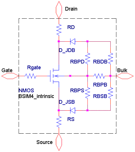
Figure 62 Schematic for the Single Transistor Model
|

|
For the single transistor model, all substrate resistance parameters RBPB, RBPD, RBPS, RBDB, and RBSB are set to fixed values for one certain device. This is the default approach, which is supported by the BSIM4 model. The description of the model in a simulator is very easy because only the call of a model card is necessary. The following netlist in spice3e2 syntax shows an example for this model description:
  .OPTIONS GMIN=1.0E-14 * *
-----------------------------------------------------------------------
* Model card for BSIM4.3.0 n-type devices | * | * Simulator: SPICE3e2 |
* Model: BSIM4 Modeling Package | * Date: 16.07.2004 | * Origin:
ICCAP_ROOT/..../bsim4/circuits/spice3/cir/nmos.cir | *
-----------------------------------------------------------------------
M1 1=D 2=G 3=S 4=B MOSMOD L=0.25u W=5u NF=1 AD=5p AS=5p PD=12u PS=12u
SA=0 SB=0 SD=0 NRD=0 NRS=0 .MODEL MOSMOD NMOS
 LEVEL = 14 VERSION = 4.3.0 BINUNIT = 2 PARAMCHK = 1 + MOBMOD = 1
 RDSMOD = 0 IGCMOD = 0 IGBMOD = 0 CAPMOD = 2 + RGATEMOD = 0 RBODYMOD = 0
TRNQSMOD = 0 ACNQSMOD = 0 FNOIMOD = 1 + TNOIMOD = 0 DIOMOD = 1
 PERMOD = 1 GEOMOD = 0
|
Fully Scalable Device
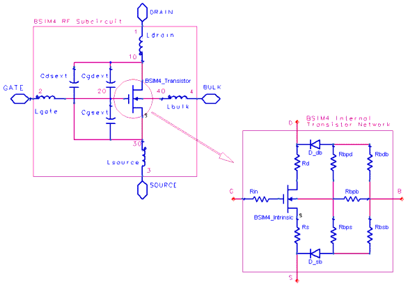
The fully scalable model has the same structure in principal as the single transistor model, but uses additional, scalable, external inductors and capacitors. It uses equations to determine the values for the substrate resistance parameters. These equations are derived from simple assumptions according to "MOS Transistor Modeling for RF IC Design" [3]. Please see the following schematic and cross section as well as the model equations for more details.
Figure 63 Scalable BSIM4 RF model
|

|
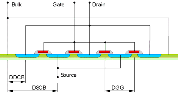
Figure 64 Cross Section of a Multifinger RF MOS Transistor
|

|
The substrate resistance network parameters RBPB, RBPD, RBPS, RBDB, and RBSB are derived using 4 new model parameters:
| • |
RSHB: sheet resistance of the substrate |
| • |
DSCB: distance between the source contact and the outer source area |
| • |
DDCB: distance between the drain contact and the outer drain area |
| • |
DGG: distance between two gate stripes |
Relevant Model Equations for Substrate Resistance Parameters
-

-

-

-

-

Substrate contact resistance scaling
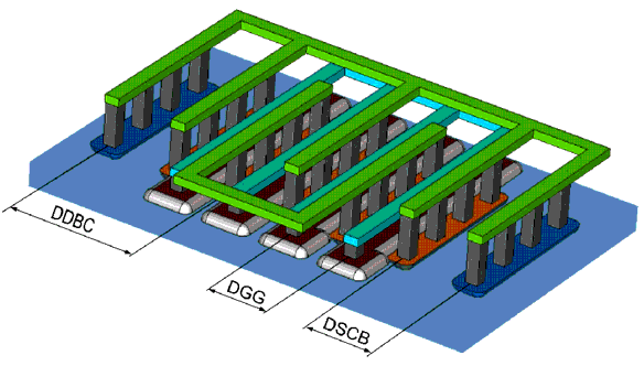
Due to different layouts of RF multifinger MOS transistors, BSIM4.3.0 has been enhanced with a new flag to model the substrate resistance according to the substrate contacts used. The flag, RSUB_EQ, can have two values:
| |
• |
RSUB_EQ = 0 : symmetric substrate contacts |
| |
• |
RSUB_EQ = 1 : horseshoe substrate contact |
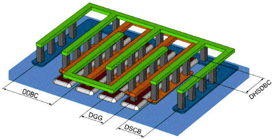
For the horseshoe contact, a new dimension has been defined, as can be seen in Figure 68:
| |
• |
DHSDBC: distance between Drain or Source edge and substrate contact of the horseshoe |
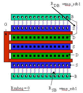
Inside the Modeling Package, temporary parameters are used to calculate the values for the five resistances used inside BSIM4. Figure 65 as well as Figure 67 are showing the use of those temporary parameters, tmp_rdb1, tmp_rdb2, tmp_rsb1 and tmp_rsb2.
The following figure shows a RF multifinger MOS transistor with symmetric substrate contacts (use RSUB_EQ = 0), whereas Figure 66 shows a 3-dimensional view of such a contact.
Figure 65 Symmetric substrate contacts, top view
|

|
Figure 66 3-dimensional view of a symmetric substrate contact with Source connected to Substrate
|

|
The following equations are used to calculate substrate resistance temporary values inside the fully scalable model:
-

-

-

-

The following figures show the horseshoe substrate contact as well as a 3-dimensional view of such a contact (use RSUB_EQ=1).
Figure 67 Horseshoe substrate contacts, top view
|

|
The temporary values calculated above are combined to give BSIM4 model parameters as follows:
RSUB_EQ = 0:


Figure 68 3-dimensional view of a horseshoe substrate contact with Source connected to Substrate
|

|
RSUB_EQ = 1:
-

-

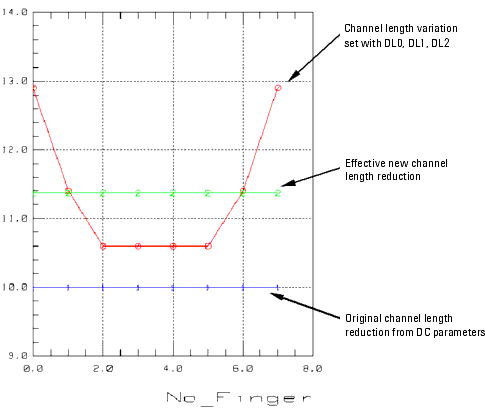
In addition, the channel length variation inside a multifinger device is not constant [4]. This behavior is taken into account using a variable channel length variation as a function of the number of gate fingers. Using the parameters DL0, DL1, and DL2 this channel length variation can be set.
Channel Length Reduction Difference
Figure 69 DL0, DL1, DL2 Channel Length Reduction Difference inside a Multifinger Device
|

|
The implementation of these enhancements requires the fully scalable model defined in a subcircuit. The following example shows the netlist implemented into the ADS simulator.
 LINK CIRC "Circuit"
{
data
{
circuitdeck
{
 ;
-----------------------------------------------------------------------------------------
 ;  Fully scalable subcircuit model for BSIM4.5.0 RF n-type devices
 ;
 ;  Simulator: Agilent Advanced Design System
 ;  Model:     BSIM4 Modeling Package
 ;  Date:      09.02.2006
 ;  Origin:    ICCAP_ROOT/..../bsim4/circuits/hpeesofsim/cir/rf_nmos_scale.cir
 ;
-----------------------------------------------------------------------------------------
 ;
 ;  --- Information for model implementation
-------------------------------------------------
 ; In ADS, call the sub circuit model as follows with the actual values of L, W, etc.
 ;
 ; BSIM4_RF_Extract:x_rf_transistor n1 n2 n3 n4 tmp_l= 0.25u tmp_w= 80u ....
 ;
 ; Please note, that according to the BSIM4 model definition, the parameters tmp_w, tmp_ad,
 ; tmp_as, tmp_pd, tmp_ps, tmp_nrs, tmp_nrd always define the TOTAL width (drain area, ...,
 ; number of drain squares) of the multi finger device.
 ; The width (drain area, ..) of a single finger of the multifinger MOSFET will be calculated
 ; inside the BSIM4 model using the instance parameter 'NF' and the selected 'GEOMOD'
parameter.
 ;
 ;
 define bsim4_rf_extract (i1 i2 i3 i4)
;--- parameters for sub-circuit -----------------------------------------------------------
 parameters tmp_l= 1u tmp_w= 10e-6 tmp_nf= 1 tmp_ad= 10e-12 tmp_as= 10e-12 tmp_pd= 22e-6
tmp_ps= 22e-6 tmp_sa= 0 tmp_sb= 0 tmp_sd= 0 tmp_nrd= 0 tmp_nrs= 0
 ;
 ;--- BSIM4 model card ---------------------------------------------------------------------
 NMOS    = 1       PMOS    = 0       VERSION = 4.50   BINUNIT = 2       PARAMCHK = 1
 MOBMOD  = 1       RDSMOD  = 0       IGCMOD  = 0      IGBMOD  = 0       CAPMOD  = 2
 RGATEMOD = 0      RBODYMOD = 0      TRNQSMOD = 0     ACNQSMOD = 0      FNOIMOD = 1
 TNOIMOD = 0       DIOMOD  = 1       PERMOD  = 1      GEOMOD  = 0       EPSROX  = 3.9
 TOXE    = 3e-9    TOXP    = 3e-9    TOXM   = 3e-9    DTOX    = 0       XJ      = 1.5e-7
 NDEP    = 1.7e17  NGATE   = 0       NSD    = 1e20    XT      = 1.55e-7 RSH     = 0
 RSHG    = 0.1     VTH0    = 0.7     PHIN   = 0       K1      = 0.33    K2      = -0.018
 K3      = 2       K3B     = 0       W0     = 2.5e-6  LPE0    = 1.74e-7 LPEB    = 0
 VBM     = -3      DVT0    = 2.2     DVT1   = 0.53    DVT2    = -0.032  DVTP0   = 0
 DVTP1   = 0.001   DVT0W   = 0       DVT1W  = 5.3e6   DVT2W   = -0.032  ETA0    = 0.08
 ETAB    = -0.07   DSUB    = 0.56    U0     = 0.067   UA      = 1e-9    UB      = 1e-19
 UC      = -0.0465 UD      = 1e+14   UP     = 0       LP      = 1e-8    EU      = 1.67
 VSAT    = 8e4     A0      = 1       AGS    = 0       B0      = 0       B1      = 0
 KETA    = -0.047  A1      = 0       A2     = 1       VOFF    = -0.08   VOFFL   = 0
 MINV    = 0       NFACTOR = 1       CIT    = 0       CDSC    = 2.4e-4  CDSCB   = 0
 CDSCD   = 0       PCLM    = 1.3     PDIBLC1 = 0.39    PDIBLC2 = 0.0086 PDIBLCB = 0
 DROUT   = 0.56    PSCBE1  = 4.24e8  PSCBE2 = 1e-5    PVAG    = 0       DELTA   = 0.01
 FPROUT  = 0       PDITS   = 1m      PDITSL = 0       PDITSD  = 0       RDSW    = 200
 RDSWMIN = 0       RDW     = 100     RDWMIN = 0       RSW     = 100     RSWMIN  = 0
 PRWG    = 1       PRWB    = 0       WR     = 1       LINT    = 0       WINT    = 0
|
  DWG     = 0       DWB     = 0       WL     = 0       WLN     = 1       WW      = 0
 WWN     = 1       WWL     = 0       LL     = 0       LLN     = 1       LW      = 0
 LWN     = 1       LWL     = 0       LLC    = 0       LWC     = 0       LWLC    = 0
 WLC     = 0       WWC     = 0       WWLC   = 0       ALPHA0  = 1e-5    ALPHA1  = 0
 BETA0   = 15      AGIDL   = 0       BGIDL  = 2.3e9   CGIDL   = 0.5     EGIDL   = 0.8
 AIGBACC = 0.43    BIGBACC = 0.054   CIGBACC = 0.075   NIGBACC = 1      AIGBINV = 0.35
 BIGBINV = 0.03    CIGBINV = 0.006   EIGBINV = 1.1     NIGBINV = 3      AIGC    = 0.54
 BIGC    = 0.054   CIGC    = 0.075   AIGSD  = 0.43    BIGSD   = 0.054   CIGSD   = 0.075
 DLCIG   = 0       NIGC    = 1       POXEDGE = 1       PIGCD   = 1      NTOX    = 1
 TOXREF  = 3e-9    XPART   = 0       CGSO   = 0       CGDO    = 0       CGBO    = 0
 CGSL    = 0       CGDL    = 0       CKAPPAS = 0.6     CKAPPAD = 0.6    CF      = 0
 CLC     = 1e-7    CLE     = 0.6     DLC    = 0       DWC     = 0       VFBCV   = -1
 NOFF    = 1       VOFFCV  = 0       ACDE   = 1       MOIN    = 15      XRCRG1  = 12
 XRCRG2  = 1       RBPB    = 50      RBPD   = 50      RBPS    = 15      RBDB    = 50
 RBSB    = 50      GBMIN   = 1e-12   RBPS0  = 50      RBPSL   = 0       RBPSW   = 0
 RBPSNF  = 0       RBPD0   = 50      RBPDL  = 0       RBPDW   = 0       RBPDNF  = 0
 RBPBX0  = 100     RBPBXL  = 0       RBPBXW = 0       RBPBXNF = 0       RBPBY0  = 100
 RBPBYL  = 0       RBPBYW  = 0       RBPBYNF = 0      RBSBX0  = 100     RBSBY0  = 100
 RBDBX0  = 100     RBDBY0  = 100     RBSDBXL = 0      RBSDBXW = 0       RBSDBXNF = 0
 RBSDBYL = 0       RBSDBYW = 0       RBSDBYNF = 0     NOIA    = 6.25e41 NOIB    = 3.125e26
 NOIC    = 8.75    EM      = 4.1e7   AF     = 1       EF      = 1       KF      = 0
 NTNOI   = 1       TNOIA   = 1.5     TNOIB  = 3.5     DMCG    = 0       DMCI    = 0
 DMDG    = 0       DMCGT   = 0       DWJ    = 0       XGW     = 0       XGL     = 0
 NGCON   = 1       XL      = 0       XW     = 0       IJTHSREV = 0.1    IJTHSFWD = 0.1
 XJBVS   = 1       BVS     = 10      JSS    = 1e-4    JSWS    = 0       JSWGS   = 0
 CJS     = 5e-4    MJS     = 0.5     MJSWS  = 0.33    CJSWS   = 5e-10   CJSWGS  = 5e-10
 MJSWGS  = 0.33    PBS     = 1       PBSWS  = 1       PBSWGS  = 1       IJTHDREV = 0.1
 IJTHDFWD = 0.1    XJBVD   = 1       BVD    = 10      JSD     = 1e-4    JSWD    = 0
 JSWGD   = 0       CJD     = 5e-4    MJD    = 0.5     MJSWD   = 0.33    CJSWD   = 5e-10
 CJSWGD  = 5e-10   MJSWGD  = 0.33    PBD    = 1       PBSWD   = 1       PBSWGD  = 1
 SAREF   = 1E-6    SBREF   = 1E-6    WLOD   = 2E-6    KU0     = 4E-6    KVSAT   = 0.2
 KVTH0   = -2E-8   TKU0    = 0.0     LLODKU0 = 1.1    WLODKU0 = 1.1     LLODVTH = 1.0
 WLODVTH = 1.0     LKU0    = 1E-6    WKU0   = 1E-6    PKU0    = 0.0     LKVTH0  = 1.1E-6
 WKVTH0  = 1.1E-6  PKVTH0  = 0.0     STK2   = 0.0     LODK2   = 1.0     STETA0  = 0.0
 LODETA0 = 1.0     LAMBDA  = 0       VTL    = 2e5     LC      = 0       XN      = 3
 TEMPMOD = 0       TNOM    = 27      UTE    = -1.5    KT1     = -0.11   KT1L    = 0
 KT2     = 0.022   UA1     = 1e-9    UB1    = -1e-18  UC1     = 0.067   UD1     = 0
 AT      = 3.3e4   PRT     = 0       TVFBSDOFF= 0     TVOFF   = 0       NJS     = 1
 NJD     = 1       XTIS    = 3       XTID   = 3       TPB     = 0       TPBSW   = 0
 TPBSWG  = 0       TCJ     = 0       TCJSW  = 0       TCJSWG  = 0       JTSS    = 0
 JTSD    = 0       JTSSWS  = 0       JTSSWD = 0       JTSSWGS = 0       JTSSWGD = 0
 NJTS    = 20.0    NJTSSW  = 20      NJTSSWG = 20     VTSS    = 10      VTSD    = 10
 VTSSWS  = 10      VTSSWD  = 10      VTSSWGS = 10     VTSSWGD = 10      XTSS    = 0.02
 XTSD    = 0.02    XTSSWS  = 0.02    XTSSWD = 0.02    XTSSWGS = 0.02    XTSSWGD = 0.02
 TNJTS   = 0       TNJTSSW = 0       TNJTSSWG= 0      LINTNOI = 0       VFBSDOFF = 0.0
 WEB     = 0       WEC     = 0       KVTH0WE = 0      K2WE    = 0       KU0WE   = 0
 SCREF   = 1E-6    WPEMOD  = 0
;
;
 model bsim4_mos BSIM4                                                               \
 NMOS     = NMOS      PMOS     = PMOS                                                \
 Version  = VERSION   Binunit  = BINUNIT   Paramchk = PARAMCHK                       \
 Mobmod   = MOBMOD    Rdsmod   = RDSMOD    Igcmod   = IGCMOD     Igbmod   = IGBMOD   \
 Capmod   = CAPMOD    Rgatemod = RGATEMOD  Rbodymod = RBODYMOD   Trnqsmod = TRNQSMOD \
 Acnqsmod = ACNQSMOD  Fnoimod  = FNOIMOD   Tnoimod  = TNOIMOD    Diomod   = DIOMOD   \
 Permod   = PERMOD    Geomod   = GEOMOD    Epsrox   = EPSROX     Toxe     = TOXE     \
 Toxp     = TOXP      Toxm     = TOXM      Dtox     = DTOX       Xj       = XJ       \
 Ndep     = NDEP      Ngate    = NGATE     Nsd      = NSD        Xt       = XT       \
 Rsh      = RSH       Rshg     = RSHG      Vth0     = VTH0       Phin     = PHIN     \
 K1       = K1        K2       = K2        K3       = K3         K3b      = K3B      \
|
  W0       = W0        Lpe0     = LPE0      Lpeb     = LPEB       Vbm      = VBM      \
 Dvt0     = DVT0      Dvt1     = DVT1      Dvt2     = DVT2       Dvtp0    = DVTP0    \
 Dvtp1    = DVTP1     Dvt0w    = DVT0W     Dvt1w    = DVT1W      Dvt2w    = DVT2W    \
 Eta0     = ETA0      Etab     = ETAB      Dsub     = DSUB       U0       = U0       \
 Ua       = UA        Ub       = UB        Uc       = UC         Ud       = UD       \
 Up       = UP        Lp       = LP        Eu       = EU         Vsat     = VSAT     \
 A0       = A0        Ags      = AGS       B0       = B0         B1       = B1       \
Keta    = KETA      A1       = A1        A2       = A2         Voff     = VOFF       \
Voffl   = VOFFL     Minv     = MINV      Nfactor  = NFACTOR    Cit      = CIT        \
Cdsc    = CDSC      Cdscb    = CDSCB     Cdscd    = CDSCD      Pclm     = PCLM       \
Pdiblc1 = PDIBLC1   Pdiblc2  = PDIBLC2   Pdiblcb  = PDIBLCB    Drout    = DROUT      \
Pscbe1  = PSCBE1    Pscbe2   = PSCBE2    Pvag     = PVAG       Delta    = DELTA      \
Fprout  = FPROUT    Pdits    = PDITS     Pditsl   = PDITSL     Pditsd   = PDITSD     \
Rdsw    = RDSW      Rdswmin  = RDSWMIN   Rdw      = RDW        Rdwmin   = RDWMIN     \
Rsw     = RSW       Rswmin   = RSWMIN    Prwg     = PRWG       Prwb     = PRWB       \
Wr      = WR        Lint     = LINT      Wint     = WINT       Dwg      = DWG        \
Dwb     = DWB       Wl       = WL        Wln      = WLN        Ww       = WW         \
Wwn     = WWN       Wwl      = WWL       Ll       = LL         Lln      = LLN        \
Lw      = LW        Lwn      = LWN       Lwl      = LWL        Llc      = LLC        \
Lwc     = LWC       Lwlc     = LWLC      Wlc      = WLC        Wwc      = WWC        \
Wwlc    = WWLC                                                                       \
Alpha0  = ALPHA0    Alpha1   = ALPHA1    Beta0   = BETA0                             \
Agidl   = AGIDL     Bgidl    = BGIDL     Cgidl   = CGIDL      Egidl   = EGIDL        \
Aigbacc = AIGBACC   Bigbacc  = BIGBACC   Cigbacc = CIGBACC    Nigbacc = NIGBACC      \
Aigbinv = AIGBINV   Bigbinv  = BIGBINV   Cigbinv = CIGBINV    Eigbinv = EIGBINV      \
Nigbinv = NIGBINV   Aigc     = AIGC      Bigc    = BIGC       Cigc    = CIGC         \
Aigsd   = AIGSD     Bigsd    = BIGSD     Cigsd   = CIGSD      Dlcig   = DLCIG        \
Nigc    = NIGC      Poxedge  = POXEDGE   Pigcd   = PIGCD      Ntox    = NTOX         \
Toxref  = TOXREF                                                                     \
Xpart   = XPART     Cgso     = CGSO      Cgdo    = CGDO       Cgbo    = CGBO         \
Cgsl    = CGSL      Cgdl     = CGDL      Ckappas = CKAPPAS    Ckappad = CKAPPAD      \
Cf      = CF        Clc      = CLC       Cle     = CLE        Dlc     = DLC          \
Dwc     = DWC       Vfbcv    = VFBCV     Noff    = NOFF       Voffcv  = VOFFCV       \
Acde    = ACDE      Moin    = MOIN                                                   \
Xrcrg1  = XRCRG1    Xrcrg2  = XRCRG2    Rbpb    = RBPB       Rbpd    = RBPD          \
Rbps    = RBPS                                                                       \
Rbdb    = RBDB      Rbsb    = RBSB      Gbmin   = GBMIN                              \
Rbps0   = RBPS0     Rbpsl   = RBPSL     Rbpsw   = RBPSW      Rbpsnf   = RBPSNF       \
Rbpd0   = RBPD0     Rbpdl   = RBPDL     Rbpdw   = RBPDW      Rbpdnf   = RBPDNF       \
Rbpbx0  = RBPBX0    Rbpbxl  = RBPBXL    Rbpbxw  = RBPBXW     Rbpbxnf  = RBPBXNF      \
Rbpby0  = RBPBY0    Rbpbyl  = RBPBYL    Rbpbyw  = RBPBYW     Rbpbynf  = RBPBYNF      \
Rbsbx0  = RBSBX0    Rbsby0  = RBSBY0    Rbdbx0  = RBDBX0     Rbdby0   = RBDBY0       \
Rbsdbxl = RBSDBXL   Rbsdbxw = RBSDBXW   Rbsdbxnf = RBSDBXNF                          \
Rbsdbyl = RBSDBYL   Rbsdbyw = RBSDBYW   Rbsdbynf = RBSDBYNF                          \
Noia    = NOIA      Noib    = NOIB      Noic    = NOIC       Em       = EM           \
Af      = AF        Ef      = EF        Kf      = KF         Ntnoi    = NTNOI        \
Tnoia   = TNOIA     Tnoib   = TNOIB                                                  \
Dmcg    = DMCG      Dmci    = DMCI      Dmdg    = DMDG       Dmcgt    = DMCGT        \
Dwj     = DWJ       Xgw     = XGW       Xgl     = XGL        Ngcon    = NGCON        \
Xl      = XL        Xw      = XW                                                     \
Ijthsrev = IJTHSREV  Ijthsfwd = IJTHSFWD  Xjbvs   = XJBVS    Bvs      = BVS          \
Jss     = JSS        Jsws    = JSWS      Jswgs   = JSWGS     Cjs      = CJS          \
Mjs     = MJS        Mjsws   = MJSWS     Cjsws   = CJSWS     Cjswgs   = CJSWGS       \
Mjswgs  = MJSWGS     Pbs     = PBS       Pbsws   = PBSWS     Pbswgs   = PBSWGS       \
Ijthdrev = IJTHDREV  Ijthdfwd = IJTHDFWD  Xjbvd  = XJBVD     Bvd      = BVD          \
Jsd     = JSD        Jswd    = JSWD      Jswgd   = JSWGD     Cjd      = CJD          \
Mjd     = MJD        Mjswd   = MJSWD     Cjswd   = CJSWD     Cjswgd   = CJSWGD       \
|
 Mjswgd  = MJSWGD     Pbd     = PBD       Pbswd   = PBSWD     Pbswgd   = PBSWGD       \
Saref   = SAREF      Sbref   = SBREF     Wlod    = WLOD      Ku0      = KU0          \
Kvsat   = KVSAT      Kvth0   = KVTH0     Tku0    = TKU0      Llodku0  = LLODKU0      \
Wlodku0 = WLODKU0    Llodvth = LLODVTH   Wlodvth = WLODVTH   Lku0     = LKU0         \
Wku0    = WKU0       Pku0    = PKU0      Lkvth0  = LKVTH0    Wkvth0   = WKVTH0       \
Pkvth0  = PKVTH0     Stk2    = STK2      Lodk2   = LODK2     Steta0   = STETA0       \
Lodeta0 = LODETA0    Lambda  = LAMBDA    Vtl     = VTL       Lc       = LC           \
Xn      = XN                                                                         \
Tempmod = TEMPMOD                                                                    \
Tnom    = TNOM       Ute     = UTE       Kt1     = KT1       Kt1l     = KT1L         \
Kt2     = KT2        Ua1     = UA1       Ub1     = UB1       Uc1      = UC1          \
Ud1     = UD1        At      = AT        Prt     = PRT       Tvfbsdoff= TVFBSDOFF    \
Tvoff   = TVOFF      Njs     = NJS       Njd     = NJD       Xtis     = XTIS         \
Xtid    = XTID       Tpb     = TPB       Tpbsw   = TPBSW     Tpbswg   = TPBSWG       \
Tcj     = TCJ        Tcjsw   = TCJSW     Tcjswg  = TCJSWG    Jtss     = JTSS         \
Jtsd    = JTSD       Jtssws  = JTSSWS    Jtsswd  = JTSSWD    Jtsswgs  = JTSSWGS      \
Jtsswgd = JTSSWGD    Njts    = NJTS      Njtssw  = NJTSSW    Njtsswg  = NJTSSWG      \
Vtss    = VTSS       Vtsd    = VTSD      Vtssws  = VTSSWS    Vtsswd   = VTSSWD       \
Vtsswgs = VTSSWGS    Vtsswgd = VTSSWGD   Xtss    = XTSS      Xtsd     = XTSD         \
Xtssws  = XTSSWS     Xtsswd  = XTSSWD    Xtsswgs = XTSSWGS   Xtsswgd  = XTSSWGD      \
Tnjts   = TNJTS      Tnjtssw = TNJTSSW   Tnjtsswg = TNJTSSWG Lintnoi  = LINTNOI      \
Vfbsdoff = VFBDSDOFF Web     = WEB       Wec     = WEC       Kvth0we = KVTH0WE       \
K2we    = K2WE       Ku0we   = KU0WE     Scref   = SCREF     Wpemod  = WPEMOD
;
;
;--- Extension to BSIM4 to enable:  -----------------------------------------
;    - scalable external capacitors taking into account cross coupling between metal lines
and
;      inductors to account for delay effects due to the size of the devices
;    - scalable channel length reduction in multi finger devices
;    - a scalable substrate network using different configurations (symmetric / horseshoe)
;    - scalable Delta L reduction
;
CGDEXT0 = 1e-9  ; external capacitance gate - drain per gate width and gate finger [F/m]
CGSEXT0 = 1e-9  ; external capacitance gate - source per gate width and gate finger [F/m]
CDSEXT0 = 1e-9  ; external capacitance drain - source per gate width and gate finger [F/m]
LDRAIN0 = 1e-6  ; drain inductance per gate width and gate finger [H/m]
LGATE0  = 1e-6  ; gate inductance per gate width and gate finger [H/m]
LSOURCE0 = 1e-6  ; source inductance per gate width and gate finger [H/m]
LBULK0  = 1e-6  ; bulk inductance per gate width and gate finger [H/m]
RSHB    = 25    ; bulk sheet resistance [Ohms sq]
DSBC    = 2e-6  ; distance source implant to bulk contact [m]
DDBC    = 2e-6  ; distance drain implant to bulk contact [m]
DGG     = 2e-6  ; distance gate to gate [m]
DHSDBC  = 2e-6  ; distance drain/source edge to horseshoe substrate contact [m]
DL0     = 0     ; basic channel length reduction correction [m]
DL1     = 0     ; channel length reduction correction 1. and 2. outer fingers [m]
DL2     = 0     ; channel length reduction correction outer fingers [m]
RSUBEQ  = 0     ; selection flag for different substrate resistance configurations [-]
                ; RSUBEQ= 0: symmetric substrate resistance contacts
                ; RSUBEQ= 1: horseshoe substrate resistance contacts
;
|
 ;--- temporary constants
#echo factor_even_odd = 0.5*(1+(tmp_nf-2*int(0.5*tmp_nf)))
#echo tmp_dl1 = (tmp_nf-4.5)/(2*abs(tmp_nf-4.5)) * 8/ tmp_nf
#echo tmp_dl2 = (tmp_nf-2.5)/(2*abs(tmp_nf-2.5)) * 4/ tmp_nf
;--- calculation of substrate resistance for different configurations
#echo tmp_rdb1 = factor_even_odd*tmp_nf*DDBC*RSHB / tmp_w
#echo tmp_rsb1 = factor_even_odd*tmp_nf*DSBC*RSHB / tmp_w
#echo tmp_rdb2 = DHSDBC*RSHB / (tmp_nf*(DGG+tmp_l))
#echo tmp_rsb2 = tmp_rdb2
#echo tmp_rdb_rsubeq0 = tmp_rdb1 ; RSUBEQ= 0  symmetric substrate contacts
#echo tmp_rsb_rsubeq0 = tmp_rsb1
#echo tmp_rdb_rsubeq1 = (tmp_rdb1*tmp_rdb2)/(tmp_rdb1+tmp_rdb2) ; RSUBEQ= 1 horseshoe
#echo tmp_rsb_rsubeq1 = (tmp_rsb1*tmp_rsb2)/(tmp_rsb1+tmp_rsb2) ; substrate contacts
#echo tmp_flag_rsubeq0 = 1/(1+abs(RSUBEQ)*1e9)   ; flag to select substrate equations
#echo tmp_flag_rsubeq1 = 1/(1+abs(RSUBEQ-1)*1e9)
#echo tmp_rbdb = tmp_flag_rsubeq0*tmp_rdb_rsubeq0 + tmp_flag_rsubeq1*tmp_rdb_rsubeq1
#echo tmp_rbsb = tmp_flag_rsubeq0*tmp_rsb_rsubeq0 + tmp_flag_rsubeq1*tmp_rsb_rsubeq1
;
; --------- Gate network ------------------------------
C:Cgdext      n20 n10 C= CGDEXT0*tmp_w
C:Cgsext      n20 n30 C= CGSEXT0*tmp_w
L:Lgate        i2 n20 L= LGATE0*tmp_w
;
; --------- Drain network -----------------------------
C:Cdsext      n10 n30 C= CDSEXT0*tmp_w
L:Ldrain       i1 n10 L= LDRAIN0*tmp_w
;
; --------- Source network -----------------------------
L:Lsource      i3 n30 L= LSOURCE0*tmp_w
;
; --------- Substrate network -------------------------
L:Lbulk        i4 n40 L= LBULK0*tmp_w
;
;--- call fully scalable MOSFET -----------------------------------------------------------
#echo bsim4_mos:M1 n10 n20 n30 n40 \
#echo Length= tmp_l - 2*(DL0+tmp_dl1*DL1+tmp_dl2*DL2) \
#echo Width= tmp_w Nf= tmp_nf Ad= tmp_ad As= tmp_as Pd= tmp_pd Ps= tmp_ps \
#echo Sa= tmp_sa Sb= tmp_sb Sd= tmp_sd \
#echo Nrd= tmp_nrd Nrs= tmp_nrs \
#echo Rbpb= 1e9 \
#echo Rbps= 0.5*RSHB*(tmp_l+DGG) / tmp_w \
#echo Rbpd= 0.5*RSHB*(tmp_l+DGG) / tmp_w \
#echo Rbsb= tmp_rbsb \
#echo Rbdb= tmp_rbdb
;
end BSIM4_RF_Extract
}
}
}
|
|
