Design Details
![]()
![]()
![]()
Design Details
|
|
|
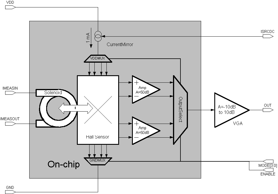
This page contains schematic details of my thesis. For a general background information behind the thesis, please see the Background page. Although it is not necessary, reading the Background page makes it easier to understand the design details described on page. Hall sensor based electric current sensor is composed of many parts. The sensor contains a solenoid, a Hall effect sensor, and the gain stage. The final current reading can be performed by a variety of voltmeters, digital multimeters(DMM) or even fancy testers. The four elements are used to make the current sensor (See figure 1). The solenoid converts the electric current to be sensed in to a magnetic field. The magnetic field is converted to a voltage via the Hall effect sensor. The hall voltage is amplified and conditioned with the gain stage. The final readout is performed by the DMM or tester. Notice that the gain stage is split between the integrated circuit and the PCB. The reasoning behind that design decision is discussed in the Gain Stage. System RequirementsBefore we perform a system anaylsis and determine the required specifications for the individual blocks, let's examine the goals of the system: It must do the following :
Items that would be nice to have, but not necessary :
Additional requirements that have been placed:
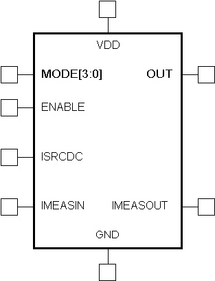
Pinout Diagram
System Block Diagram
Pin Description
Block Diagram Description
Gain Block CalculationsWith those points in mind, let's tackle the 1V/1A sensitivity issue. This means that at minimum 1mA current would produce a 1mV signal -- most test equipment should be able to sense this signal. The following table contains typical values of gains for the solenoid, hall sensor. It also shows the required gain.
Note that the Hall sensor and Solenoid gain parameters were estimated from past papers and from classical magnetic theory calculations (i.e Maxwell Equations). Noise Calculations.Since the most of the sensors generate a very low signal strength, noise from transistors and resistors become an important fact. From our requirements, we require 1mA of accuracy. We shall assume the Solenoid is noiseless since the series resistance is low (<0.25 ohms) and reactive elements is considered noiseless. The Hall sensor has a source resistance of 1kohm; thus, the Hall sensor will have thermal noise contribution from the source resistance. The gain stage will also contribute noise in the form of noise figure (NF). The following table is the noise power budget calculations (F = 10kHz, T= 300K):
From the table above, there is a 5.82dB margin for noise. The margin should be sufficient to other minor factors.
|
|
Copyright ©2000.
|