Hall Effect Sensor
![]()
![]()
![]()
Hall Effect Sensor
|
|
|
IntroductionThe Hall Effect sensor is a magnetic field sensor. It measures directional magnetic fields and translates it in to a voltage, known as Hall voltage. The effect is based on charges that move through a semiconductor but the charges are deflected by a magnetic field. The deflection is caused by the Lorentz force. The deflection is very small, however it is large enough to create a small voltage, or Hall voltage, to form along the edge of the semiconductor (see figure 1).
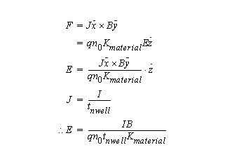
Figure 1 : Basic Hall Element. Note that it is essential that a semiconductor be used as a Hall element, because semiconductors have a higher carrier velocity than other metals. "Low doped semiconductor material possess a low density of quasi-free chage carriers. The carriers hardly interact with the crystal lattice, which gives them a high mobility."[1] Due to the low density, "we can a apply a higher electric drift field without thermally degenerating the material."[1] Higher carrier velocity results in larger Lorentz force for a given magnetic field, which in turn increases the magnetic field to Hall voltage gain. Mathematic DerivationTo understand how the Vhall formula was calculated, let's assume current is flowing uniformly through a block of material. If a magnetic field is perpendicular to the current, the electrons within the current will experience the Lorentz force. The Lorentz force is define by formula 2 and its direction is perpendicular to the current and the magnetic field. The force experience by each electron is shown in formula 3. If each passing electron was subject to the Lorentz force, electrons will accumulate on face of the block. The greater the applied Lorentz force, the more electrons the face of the block will accumulated. The electron accumulation on to one side of the block will generate a electric field(4). The electric field in turn generates a voltage potential than can be measured(5).
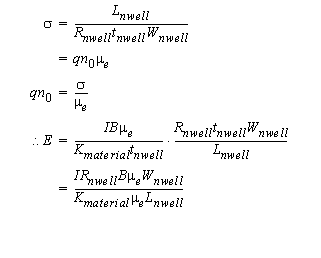
N-Well Hall ElementOur design will use a N-Well based Hall Element. N-Well is a n-doped region within a silicon wafer substrate. Usually, the N-well is used to as a substate for the PMOS structure. However in our situation, we will use it as our sensor that is a lightly n-doped region (n-). With the N-Well structure, we can simplify equation 5 by assuming that the N-well is lightly dope. By assuming that information, we can say several things. The conductivty of the N-well structure in Figure 3 is given in formula 6.
From the conductivity equations, we can substitute the parameters in to reduce the Hall element equation (1). Thus, the Hall voltage that is generated is only related to four parameters - the current flowing through the Hall element, the resistance of the Hall element, the mobility of the Hall element and the field perpendicular to the Hall element. Lightly dope N device is the proper type to use in the Hall element because it has higher mobility than other device and N-Wells are one of the most resistive per unit area. Thus, N-well is the proper choice. Notice that the current flowing through the element and resistance of the N-well can be further collapsed in to the voltage across the current inputs of the element via Ohm's law. Hence the gain of the Hall element will be limited by the voltage one can place across the current inputs, the mobility of the N-well, the dimensions of the N-Well and the Magnetic Field strength. The material constant (Kmaterial) has been experimentally and analytically calculated to be 1.18 for silicon [1]. Due to the lengthy derivations involved with the material constant, this material is not included on this web page. The only parameter that we have full control over is the N-well dimensions. For ease of analysis and circuit layout, the width and length of the N-well are the same. Plug-In the NumbersFrom final N-well hall sensor equation, we can deduce the theoretical gain of our proposed sensor. Typical n- doped silicon has a mobility of 1340 cm2/V at 300K or room temperature. In general, mobility degrades as room temperature increases. Modern circuits will use appropriate circuitry to compensate for temperature variations. Since the thesis is a proof of concept, compensation circuitry may be included in the final design if time is permitting. In a typical CMOS process with p- substrate, N-well usually have a sheet roll resistance of 1000 ohms/square. Since are design assumes a square hall sensor, the resistance of the sensor is 1000 ohms. Typically, N-well sheet resistance is not very well controlled in CMOS fabrication. Thus, N-well sheet roll resistance can change as much as +/-40%. In addition, N-well do not have well controlled geometry. Geometry variations may affect the overall resistance of the N-well if the device is too small. This effect is similar to matching transistors that are minimum geometry. Thus, a large geometry N-well device should be used to help reduce this effect. As a result, the final gain of the proposed sensor is 0.237 mV/T if a nominal bias current of 1.5mA is used. We will use this gain throughout the system level calculations and for calculating the necessary gain required by other stages to make this signal useful.
|
|
Copyright ©2000.
|