Background
![]()
![]()
![]()
Background
|
|
|
The basic principle in the thesis is to use Hall Effect Sensors to measure current flowing through wires. The key problem is whether it is possible to integrate the Hall sensor within the same substrate as the device under test (DUT). Discussion below will introduce you to the Hall effect. Later discussion will describe how one could integrate it on to an CMOS IC. Current Methods of Measuring CurrentThe ability to measure current flow within an integrated circuit has been a useful too to help improve the testability of VLSI chips. In production testing of VLSI chips, chips are run through a series of tests to elminate the non-funcational and out of specification chips. Tests such as funcational test and quiesent current testing (IDDQ) are used in these situations. An emerging test is online current testing. Online current testing involves monitoring the current consumption of individual blocks within the VLSI chips when a series of test patterns are passed through the blocks-under-test (BUT). The current consumption is recorded and compared to an ideal simulation via a circuit simulator. If the current consumption signature differs drastically between the BUT and the simulated results, the BUT has failed the test. This test methodology works very well, but the test relies on the ability to measure current within the chip. One might argue that measure current consumption from an external pin may be suffice. For small designs, an external pin measurement may be done. But for VLSI chips, such as the Intel Pentium III with 35+ million gates, it just won't work. Generating the "ideal" current signature for the Pentium III would take years if at all possible. Having "dedicated" pins to measure key blocks within the IC are not acceptable solutions in real production chips because pins are a scarce resource. Thus, the current sensor must be placed inside the IC. The traditional technique of sensing current is using Ohm's Law. A resistive device, such as a transistor or a resistor, is placed in series with the BUT's power supply. Any current drawn from the BUT will be drawn through the resistive device. Ohm's law states that V=IR; thus, the voltage drop across the resistor is proportional to the current drawn by the BUT. The main problem with this sensor is that it reduces the working voltage of the BUT. In 5V power VLSI, this may not be a problem. But a growing trend to use lower power supplies, such as 1.8V, make this technique very difficult to implement without affecting the BUT. In addition, large current drawing BUTs require very small resistors. These resistors can disappate heat over time. It is also a known fact that very small resistors are not very accurate due to their size and process limitation. This project proposes a different current sensing device. It is a device based on the Hall effect, and it solves many of the problems illustrated above. Hall EffectThe Hall effect was discovered by Edwin Hall in 1879. The effect is based on charges that move through a semiconductor but the charges are deflected by a magnetic field. The deflection is caused by the Lorentz force. The deflection is very small, however it is large enough to create a small voltage, or Hall voltage, to form along the edge of the semiconductor (see figure 1).
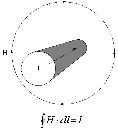
Figure 1 : Basic Hall Element. Note that it is essential that a semiconductor be used as a Hall element, because semiconductors have a higher carrier velocity than other metals. "Low doped semiconductor material possess a low density of quasi-free chage carriers. The carriers hardly interact with the crystal lattice, which gives them a high mobility."[1] Due to the low density, "we can a apply a higher electric drift field without thermally degenerating the material."[1] Higher carrier velocity results in larger Lorentz force for a given magnetic field, which in turn increases the magnetic field to Hall voltage gain. Magnetic FieldMagnetic fields are generated by any conductor with flowing current. The magnetic field strength is proportional to the current, but it is inversely proportional to the distance from the conductor. The above property is summarized by the Ampere's Law (see figure 2). As a result, the SI units for magnetic field is ampere per meter (A/m). A field strength of 1 A/m is equivalent to a magnetic field generated by a cylinderacle conductor that carries 1A and is 1m away.
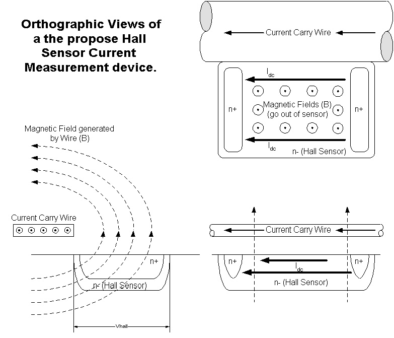
The Project.When you combine Ampere's Law and Hall element, a current sensing device is formed (See figure 3). In the figure below, a metal wire is carry Im current. Based on Ampere's Law, a current carrying wire will induce a magnetic field around the condutor. If a magnetic field sensor, such as a Hall element, is placed near the conducting wire, then the Hall element can measure the field strength induced by the conductor. Since the field strength is proportional to the current passing through the conductor, the Hall element can measure the Im current.
Figure 3 depicts a practical implementation for an on-chip Hall Current Sensor. The Hall sensor resides in a light n dope silicon (Si) substrate called an N-well. Modern silicon substrates are usually lightly p doped, so ion implantation is used to locally change the substrate from light dope p to lightly dope n. These local changes are called N-wells. In a modern CMOS process, the N-well is used to form the PMOS transistor. NMOS transistors reside on the p- substrate. Since it is desireable to use higher mobility materials for the Hall sensor, the N-well was the appropriate choice (N-well's majority carriers are electrons). N+ deposits are place on the ends of the N-well to improve conductivity between metals and the N-well. Since Idc current must pass through the N-well and Idc current comes from an external source (usually delivered by a metal layer), good conductivity is required between metal and silicon (i.e. n-well). Once current is flowing through the N-well via the N+ deposits and a magnetic field is passing through the N-well, a Hall voltage (Vhall) will be formed. In this implementation, optimal measurement of the magnetic field is when the field is normal to the surface of the silicon semiconductor. If magnetic fields pass through the N-well based Hall sensor at an arbitrary angle, only the component that is normal to the surface will be measured. The other two components are ignored. This is the basic idea behind the project. Other parts of this web site will explore the mathematics, the physics and the practicality of the CMOS Hall current sensor. Practical Improvements.The sensor, as shown above, works in principal. However, additional improvements must be made to make it more accurate and more sensitive. As we have discussed before, the Hall effect is very small signal effect. A typical current sensor gain of 30mA/A -- making it difficult to measure current below 10mA. Another problem is that the sensor resides on a CMOS substrate that is not very well controlled. Process and temperature variations change key parmeters used by the sensor, such as mobility and doping densities. Stray magnetic fields from external sources and surounding current carrying wires could affect the sensor's ability to give accurate readings. These issues must be solved before this sensor can be used in practical applications. Small Sensor GainTypically, a hall element will have a gain of 300uV/Guass or 3V/T. But, typical magnetic fields generated by a 1A wire at a distance of 5um (the approximate distance between the wire and the centre of the sensor) is about 10mT. The overall gain of the current sensor is 30mV/A. The low gain makes the propose device difficult to measure on-chip current below 10mA. Current consumption within the 10mA range is not uncommon within modern CMOS circuits, so improvements must be made to increase the sensitivity. Increase the Magnetic Field.One way of increasing the gain is to increase the gain of the current to magnetic field conversion. Since Ampere's Law is govern by physical properties, it would be impossible to change the actual law. It is possible to increase the gain and still obey Ampere's law. One approach is to form a loop or a single loop solenoid. The magnetic fields generated by a solenoid is much larger than those generated by a infinitely long wire. The gain would increase from 10mT/A to 29mT/A. The 3x improvement places the overall gain to 90mV/A. By increasing the number of loops the solenoid has, the gain of the overall current sensor will increase proportionally. On-Chip GainAnother way to increase the sensor's gain is to amplify the output of the sensor. At first, one would believe this is a simple task. Unfortunately, there are some problems with this technique. Ideal amplifiers just boost the input by a known factor. Practical amplifiers also boost the input by a known factor, but the gain factor may vary (for example, the intended gain of the amplifier could be 10x, but the measure gain could be 10.1x). Practical amplifiers have power supply rejection problems. Power supply rejection is measuring the gain between the power supply and the output. The higher the power supply rejection is, the lower the gain is. High power supply rejection is very desireable, since most microchip power supplies are very noisy. The worst problem with ideal amplifiers is input offsets. Large input offsets (>10mV) cause the amplifier to percieve a 10mV DC component on the input. If your signal is only 1mV, then the amplifier will think it is receiving a 11mV signal at the input. If the signal is amplified by 100 times, the input AND the offset will be amplified. Thus, the amplified signal will distorted by the extra DC component. This is highly undesireable and the input offsets vary over time and process. The first two problems are solved by using good amplifier circuits. A good differential, such as a folded-cascode, amplifier with good power supply rejection would be sufficent for this amplification. The input offset issue is not an easy problem to solve. The typical solution is to use chopper-stabalized differential amplifiers. Chopper-stabalized amplifiers are nosier than the typical linear amplifier due to switching noise generated by the chopper.
|
|
Copyright ©2000.
|