Wada's model contains a gate-level decoder model without any parasitic capacitances or resistances. It also assumes all memory sub-arrays are stacked single file in a linear array. We have used a detailed transistor-level decoder that includes both parasitic capacitances and resistances. We have also assumed that sub-arrays are placed in a two-dimensional array to minimize critical wiring parasitics.
Figure 3 shows the logical structure of the decoder architecture used in this model. The decoder in Figure 3 contains three stages. Each block in the first stage takes three address bits (in true and complement), and generates a 1-of-8 code, driving a precharged decoder bus. These 1-of-8 codes are combined using NOR gates in the second stage. The final stage is an inverter that drives each wordline driver. We also model separate decoder driver buffers for driving the 3-to-8 decoders of the data arrays and the tag arrays.
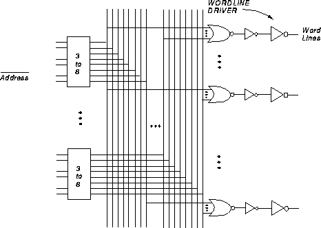
Figure 3: Single decoder structure
Estimating the wire lengths in the decoder requires knowledge of the memory
tile layout. As mentioned in Section 3, the memory is
divided into ![]() subarrays; each of these arrays is
subarrays; each of these arrays is
![]() cells wide. If these arrays were placed
side-by-side, the total memory width would be
cells wide. If these arrays were placed
side-by-side, the total memory width would be ![]() cells. Instead, we assume they are grouped in two-by-two blocks, with the
3-to-8 predecode NAND gates at the center of each block;
Figure 4 shows one of these blocks. This reduces the
length of the connection between the decoder driver and the predecode block to
approximately one quarter of the total memory width, or
cells. Instead, we assume they are grouped in two-by-two blocks, with the
3-to-8 predecode NAND gates at the center of each block;
Figure 4 shows one of these blocks. This reduces the
length of the connection between the decoder driver and the predecode block to
approximately one quarter of the total memory width, or
![]() . The length of the connection between the
predecode block and the NOR gate is then (on average) half of the
subarray height, which is
. The length of the connection between the
predecode block and the NOR gate is then (on average) half of the
subarray height, which is ![]() cells.
In large memories with many groups the bits in the
memory are arranged so that all bits driving the same data output bus are in
the same group, shortening the data bus.
cells.
In large memories with many groups the bits in the
memory are arranged so that all bits driving the same data output bus are in
the same group, shortening the data bus.
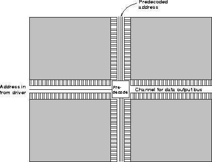
Figure 4: Memory block tiling assumptions