Print version of this Book (PDF file)
ADS Parameter Sweeps
When using the ADS simulator in IC-CAP, the method of specifying parameter sweeps differs between performing single device simulations and circuit simulations.
Device Simulation Parameter Sweep
To sweep a parameter in an ADS device simulation:
| 1 | Add an input specification of mode P to the Setup. Enter the name of the parameter as it appears in the Parameters table. |
| 2 | Enter the sweep type and values. |
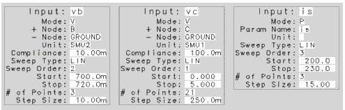
The Device Simulation Parameter Sweep example uses the hpsimnpn.mdl model with an input of mode P to the fearly setup. This input specifies a linear sweep of the parameter from 200.0e-15 to 230.0e-15 amperes in steps of 15.0e-15 amperes.
Figure 19 ADS Device Simulation Parameter Sweep Setup Example
During the simulation, IC-CAP generates the following input deck.
 Options\
  ASCII_Rawfile=no UseNutmegFormat=yes
; Simulation Input File for BJT

model npn BJT NPN=yes  \
Is =  2.704E-16  \
Bf =  86.16  \
Nf =  0.979  \
Vaf =  86.95  \
Ikf =  0.01491  \
Ise =  1.886E-14  \
Ne =  1.522  \
Br =  8.799  \
Nr =  0.9967  \
Var =  9.757  \
Ikr =  0.02369  \
Isc =  1.095E-15  \
Nc =  1.1  \
Rb =  8.706  \
Irb =  0.001509  \
Rbm =  5.833  \
Re =  1.385  \
Rc =  10.68  \
Xtb =  0  \
Eg =  1.11  \
Xti =  3  \
Cje =  1.312E-12  \
Vje =  0.6151  \
Mje =  0.2052  \
Tf  =  4.781E-11  \
Xtf =  4.359  \
Vtf =  3.237  \
Itf =  0.01753  \
Ptf =  176.2  \
Cjc =  1.394E-12  \
Vjc =  0.5428  \
Mjc =  0.2254  \
Xcjc =  1  \
Tr  =  5.099E-09  \
Cjs =  1.004E-13  \
Vjs =  0.5668  \
Mjs =  0.2696  \
Fc =  0.5  \
Tnom =  27
npn:devckt 1 2 3 4
; START SOURCES
V_Source:VBGROUND 2 0 Vdc=0
V_Source:VCGROUND 1 0 Vdc=0
V_Source:VEGROUND 3 0 Vdc=0
V_Source:VSGROUND 4 0 Vdc=-3
; END SOURCES
SweepPlan:swp1 Start=0 Stop=5 Step=0.25
SweepPlan:swp2 Start=0.7 Stop=0.72 Step=0.01
DC:dc1 SweepPlan=swp1 SweepVar="VCGROUND.Vdc"
ParamSweep:ct1 SimInstanceName="dc1" SweepPlan=swp2
SweepVar="VBGROUND.Vdc"
Circuit Simulation Parameter Sweep
Specifying a parameter sweep for a circuit simulation requires a different approach from a parameter sweep for a device simulation.
To sweep a parameter in an ADS circuit simulation:
| 1 | Specify a global variable in the ADS circuit description and set it to an initial value. |
| 2 | Set the value of the parameter in the circuit description equal to the global variable name. |
| 3 | Add a variable in IC-CAP with the same name as the global ADS parameter. |
| 4 | Add an input specification of mode P to the Setup. |
| 5 | Enter the global variable name in the Name field of the Input table. |
| 6 | Enter the sweep type and values. |
Example Circuit Simulation Parameter Sweep
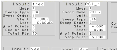
The Circuit Simulation Parameter Sweep example, uses a model for opamp simulation. The following line is included with the circuit description:
This complete circuit description is shown below.
 ;Simulation Input File in hpeesofsim Input Deck Format

global RC1_r=4352

define opamp1 (2 3 4 6 7)
; Internal OpAmp circuit
; using Boyle-Pederson Macro Model
; Input differential amplifier
NPN1:Q1 10 2 12
NPN2:Q2 11 3 13
model NPN1 BJT NPN=yes \
Is = 8E-16 \
Bf = 52.81
model NPN2 BJT NPN=yes \
Is = 8.093E-16 \
Bf = 52.66
R:RC1 7 10 R=RC1_r
R:RC2 7 11 R=4352
C:C1 10 11 C=4.529E-12
R:RE1 12 14 R=2392
R:RE2 13 14 R=2392
R:RE 14 0 R=7.27E+06
C:CE 14 0 C=7.5E-12
; Power dissipation modeling resistor
R:RP 7 4 R=1.515E+04
; 1st gain stage
#uselib "ckt", "VCCS"
VCCS:GCM 14 0 0 15 G=1.152E-09
VCCS:GA 10 11 15 0 G=0.0002298
R:R2 15 0 R=1E+05
; Compensation capacitor
C:C2 15 16 C=1E-11
; 2nd gain stage
VCCS:GB 15 0 16 0 G=37.1
R:RO2 16 0 R=489.2
DMOD1:D1 16 17
DMOD1:D2 17 16
model DMOD1 Diode \
Is = 3.822E-32
R:RC 17 0 R=0.0001986
VCCS:GC 6 0 0 17 G=5034
; Output circuit
R:RO1 16 6 R=76.8
DMOD2:D3 6 18
DMOD2:D4 19 6
model DMOD2 Diode \
Is = 3.822E-32
V_Source:VC 7 18 Vdc=1.604
V_Source:VE 19 4 Vdc=3.104
; Input diff amp bias source
I_Source:IEE 14 4 Idc=2.751E-05
end opamp1

define inv_amp (1 2 3 4 6 7 )
opamp1:X1  2 3 4 6 7
R:Rf  6 2 R=1E+004
R:Rin  2 1 R=2000
R:Rgnd  3 0 R=0.001
end inv_amp

inv_amp:XCKT n1 n2 n3 n4 n5 n6
; START SOURCES
V_Source:V1GROUND n1 0 Vdc=0 Vac=polar(1,0)
V_Source:V7GROUND n6 0 Vdc=15
V_Source:V4GROUND n4 0 Vdc=-15 ; END SOURCES
R:RO2 n2 0 R=100MEG
R:RO3 n3 0 R=100MEG
R:RO5 n5 0 R=100MEG
SweepPlan:swpfreq Start=1000 Stop=1e+07 Dec=3
SweepPlan:swp1 Start=4 Stop=10 Step=6
AC:ac1 SweepPlan=swpfreq SweepVar="freq"
ParamSweep:ct1 SimInstanceName="ac1"
SweepPlan=swp1 SweepVar="RC1_r"
In this example, the value of R:RC1 is set to RC1_r. You must also add a variable called RC1_r to the IC-CAP model variables table and set the variable to a value, such as, 4.000K. In the example model, you must then add an input call RC1_r to the setup . The Inputs table is shown in the following figure.
Figure 20 ADS Circuit Parameter Sweep Setup Example
For additional information on sweeping parameters, refer to "Specifying Parameter or Variable Sweeps" in the User's Guide.
The following sections of this chapter describe in detail the syntax for the ADS Simulator.
Using LSYNC sweeps
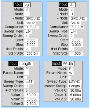
When you use LSYNC sweeps for an ADS simulation, data is written to a data access component file. This file contains the synchronized lists and the specific elements in the netlist that refer to LSYNC values. These elements are accessed using variables and an index.
A single sweep for the LSYNC group is then created to sweep the index.
 Options ASCII_Rawfile=no UseNutmegFormat=yes

model nmos3 MOSFET nmos=yes \
UO          = 1000      \
Vto         = 1.136     \
Nfs         = 0         \
Tox         = 1E-007    \
Nsub        = 5.31E+015 \
Nss         = 0         \
Vmax        = 1E+006    \
Rs          = 0         \
Rd          = 0         \
Rsh         = 0         \
Cbd         = 0         \
Cbs         = 0         \
Cj          = 0         \
Mj          = 0.5       \
Cjsw        = 0         \
Mjsw        = 0.33      \
Is          = 1E-014    \
Pb          = 0.8       \
Fc          = 0.5       \
Xj          = 9.438E-008 \
Ld          = 2.955E-007 \
Delta       = 0.9338    \
Theta       = 0.04124   \
Eta         = 0         \
Kappa       = 0.2

nmos3:devckt n1 n2 n3 n4 L = lsync0_0 W = lsync0_1 Ad = 1e-10
As = 1e-10 Pd = 0.000104 Ps = 0.000104 ; START SOURCES
V_Source:VGGROUND n2 0 Vdc=0 V_Source:VBGROUND n4 0 Vdc=0
V_Source:VDGROUND n1 0 Vdc=0.1 V_Source:VSGROUND n3 0 Vdc=0
; END SOURCES

INDEX0=0
#uselib "ckt" , "DAC"
DAC:DAC0 File="c:\ictmp\IC19_lsync0" Type="dscr"
InterpMode="index_lookup" iVar1=1 iVal1=INDEX0

lsync0_0=file {DAC0, "lval0"}
lsync0_1 = file {DAC0, "lval1"}
SweepPlan:swp1 Start=0 Stop=5 Step=0.2
SweepPlan:swp2 Start=-3 Stop=0 Step=1.5 Reverse=yes
SweepPlan:swp3 Start=0 Stop=2 Step=1
DC:dc1 SweepPlan=swp1 SweepVar="VGGROUND.Vdc"
ParamSweep:ct1 SimInstanceName="dc1" SweepPlan=swp2
SweepVar="VBGROUND.Vdc"
ParamSweep:ct2 SimInstanceName="ct1" SweepPlan=swp3
SweepVar="INDEX0"
And the contents of IC19_lsync0 will be:
 BEGIN DSCRDATA
 % INDEX0 lval0 lval1
 0 5e-05 5e-05
 1 5e-05 5e-06
 2 2.5e-06 5e-05