Print version of this Book (PDF file)
Functional Circuit Blocks
Previous sections in this chapter provided different aspects of the use of IC-CAP for modeling complete functional circuits. This section provides detailed examples of circuit models and custom model extractions you can create. These examples are provided to stimulate ideas for using IC-CAP to meet specific circuit modeling requirements.
Types of Circuits in IC-CAP
The types of circuits for measurement and simulation with IC-CAP are unlimited. Anything that can be simulated on a stand-alone SPICE simulator can be simulated with IC-CAP. In fact, any type of system that can be measured with the IC-CAP library of instruments can be characterized.
With the variety of components supported by SPICE, IC-CAP can be used to both characterize and design circuit modules. Classical examples of both single device and functional circuit modeling problems that are easily solved with IC-CAP are included.
Modeling the Reverse Active Region of an NPN Transistor
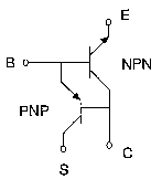
One of the constant sources of error in modeling the performance of a reverse active NPN transistor is the parasitic PNP formed by the base, collector, and substrate of the integrated structure. (This was briefly described in PNP Transistors.) A simple solution to modeling this region of operation is to use the complete functional circuit displayed in the following figure.
Figure 222 NPN Transistor with Parasitic PNP
Model file npnwpnp.mdl is included as an example of solving this problem. It has a single DUT/Setup that measure and model the reverse active operation of an NPN transistor.
The previous figure shows that the emitter of the PNP steals current from the base terminal of the NPN. The single dominant parameter that models this PNP current flow is the saturation current IS. (Modeling the transistor at this point assumes that the DC NPN parameters have already been obtained using another model file. The bjt_npn.mdl model file has a complete set of DUTs and setups to perform this. For more information, refer to Chapter 8, "Bipolar Transistor Characterization.")
The rgummel setup then uses an optimize function to simultaneously extract the reverse active NPN parameters BR, IKR, ISC, and NC and the PNP parameter IS. The optimization proceeds by simulating the compound device, which is represented as a 2-transistor circuit, and numerically adjusting these model parameters.
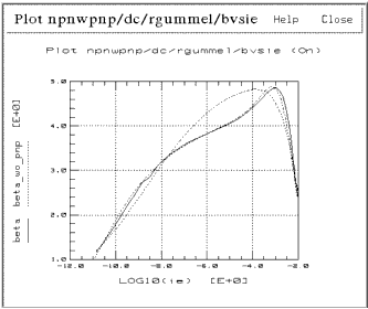
The plot in the following figure is of reverse beta versus emitter current. It includes the simulation of the single transistor reverse model and measurement and simulation of the 2-transistor compound structure. The result of this extraction is a near perfect agreement between measured and simulated data. Also examine the resulting magnitudes of both IS (large enough to not be negligible) and BR (much higher than for a single device extraction). This example shows the improvement you can attain in using a full circuit description to model an integrated device structure.
Figure 223 Reverse Beta versus Ie for Single NPN and Compound NPN-PNP Structure
Modeling an Operational Amplifier
The operational amplifier is included with IC-CAP as an example of how to do relatively complex macro modeling. It illustrates the simplification of a complex circuit to the necessary and sufficient components that enable it to be accurately represented. This model includes a Program transform that extracts model parameters from data sheet specifications of its performance. The inputs to this transform could also be measurements of the opamp's electrical characteristics. This same Program transform has also been converted into a standard IC-CAP function by writing it in the C programming language (in the userc.c module) and compiling and linking it into the system. The circuit chosen follows the model developed by Boyle, Cohn, Pederson, and Solomon [1]. This circuit model is in the opamp.mdl example file.
Opamp Macro Model
The stages in this opamp model are: non-linear differential input, intermediate linear gain, and output driver. These enable most of the possible operating regions of the complete circuit to be adequately simulated.
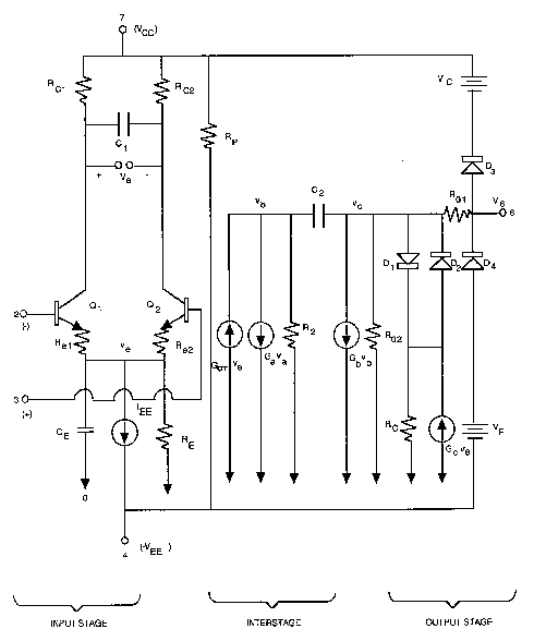
The input stage contains transistors Q1 and Q2 connected as a differential amplifier, biased with a fixed current source (see Figure 223). Q1 and Q2 provide both differential mode (DM) and common mode (CM) characteristics. Passive components in the input stage provide slew rate effects (C2, Ce, Re1, Re2), 0dB frequency control (Rc1, Rc2), DM excess phase (C1), and CM input resistance (R1).
The intermediate gain stage provides linear amplification through voltage controlled current sources Ga, and Gb, which model the differential gain of the opamp. Capacitor C2 controls the dominant pole. CM gain is modeled with the voltage controlled source that has the coefficient Gcm.
In the output stage, AC and DC output resistances are modeled with Ro1 and Ro2. Output drive voltage is supplied through diodes D1 and D2 and voltage controlled voltage source (Gc*v6*Rc). The independent voltage sources in series with diodes D3 and D4 clamp the opamp under conditions that would force the output voltage to one of the supply rails.
The development of this opamp model uses the concepts of simplification and buildup to reduce the number of active and passive components. For example, to maintain non-linear effects the input stage has been simplified to two transistors, and an independent current source has been substituted for the usual bias circuitry. In the interstage amplifier, buildup is used to emulate a circuit characteristic through alternate circuitry. The stage is modeled by two voltage controlled current sources and a capacitor for compensation. These techniques take a piece-by-piece approach to the development of a model. They can be applied to virtually any circuit or subcell.
Opamp Circuit Model
The following figure shows the macro model that represents the full opamp circuit, followed by circuit elements in order from the input to the output stage. Figure 225 shows the complete opamp model circuit definition used in this example.
Figure 225 Opamp Circuit Diagram
Inputs to the Opamp Macro Extraction
Inputs to the opamp model extraction describe its electrical performance. These characteristics can be measured on actual devices or obtained from data sheet specifications. Due to the flexibility of the origin of the inputs, you can experiment with the opamp's performance as it relates to the model elements that control it. The following table lists the inputs to the opamp extraction.
Extraction Equations for the Opamp Macro Model
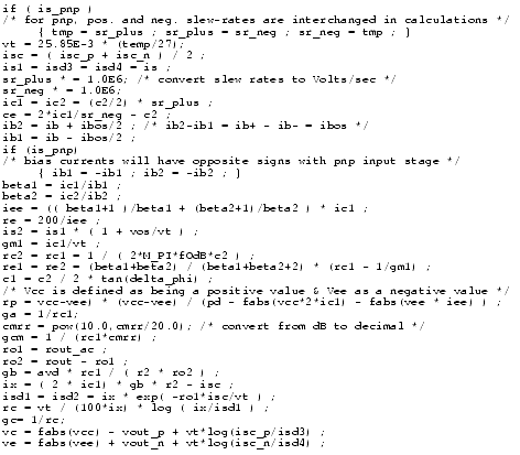
The inputs to the macro model extraction described are used by the set of equations shown in the following figure to produce the model parameters. These equations are programmed into the userc.c module exactly as shown.
Because of the simplicity of the equations, they can also be entered into a Program transform using the Parameter Extraction Language. This allows experimentation with model extraction techniques before coding the final extraction in C and linking it to IC-CAP. This has been done with the opamp macro model to provide a typical example of writing custom model extractions.
Figure 226 C Coded Opamp Extraction Equations
Bias Circuitry
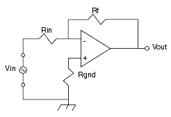
The opamp model, fully defined and model parameters extracted, can now be used as a functional circuit block. This requires that the opamp be biased with external supply voltages and circuit configuring components. This was demonstrated previously through the use of a test circuit. The test circuit implemented forms an inverting amplifier using an input and feedback resistor with the opamp. This results in a complete functional circuit whose performance can be studied in more detail. The test circuit definition and the resulting equivalent circuit are shown in the following 2 figures.
Figure 227 Test Circuit Definition to Form an Inverting Amplifier
 * Inverting Amplifier
.SUBCKT  inv_amp 1 2 3 4 6 7
X1  2 3 4 6 7  opamp_1
Rf    6  2  10K
Rin   2  1  2K
Rgnd  3  0  1.0m
.ENDS
Figure 228 Equivalent Schematic of Opamp in Inverting Amplifier
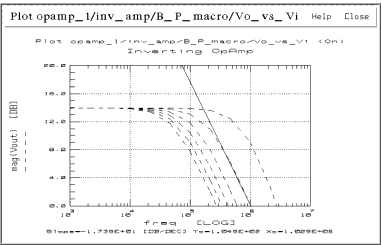
The plot in the following figure illustrates how this functional circuit can be studied. The opamp circuit has been simulated with the compensation capacitance used as one of the sweep parameters. The AC voltage gain is plotted versus frequency with steps of different values of C2. The diagonal line is the break point between process limitations and circuit limitations. To increase frequency response, the internal capacitor on the chip (nominal 30pF) would have to be reduced. To force earlier roll-off, more external capacitance can be added. This analysis indicates the range of gain-bandwidth product available for different values of capacitance. Similar analyses can be performed for any area of this circuit's operation.