Print version of this Book (PDF file)
MNS Parameter Sweeps
When using the MNS simulator in IC-CAP, the method of specifying parameter sweeps differs between performing single device simulations and circuit simulations.
Device Simulation Parameter Sweep
To sweep a parameter in an MNS device simulation:
| 1 | Add an input specification of mode P to the Setup. Enter the name of the parameter as it appears in the Parameters table. |
| 2 | Enter the sweep type and values. |
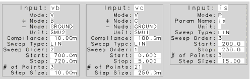
The Device Simulation Parameter Sweep example uses the mnsnpn.mdl model with an input of mode P to the fearly setup. This input specifies a linear sweep of the parameter from 200.0e-15 to 230.0e-15 amperes in steps of 15.0e-15 amperes.
Figure 16 MNS Device Simulation Parameter Sweep Setup Example
During the simulation, IC-CAP generates the following input deck.
 ; Simulation Input File options ascii=no
model mnsnpn bjt npn=yes\
is=4.015E-16\
bf = 60 \ nf = 0.9955\
 vaf = 84.56\
 ikf = 0.01195 \
 ise = 3.405E-14 \
 ne = 1.594 \
 br = 10.79 \
 nr = 1.002 \
 var = 9.759 \
 ikr = 0.00237 \
 isc = 1.095E-15 \
 nc = 1.1 \
 rb = 9.117 \
 irb = 0.001613 \
 rbm =5.62 \
 re = 1.385 \
 rc = 9.292 \
 xtb = 1.7 \
 eg = 1.11 \
 xti = 3 \
 cje = 1.312E-12 \
 vje = 1.11 \
 mje = 0.3475 \
 tf = 5.274E-11 \
 xtf = 5.625 \
 vtf = 2.678 \
 itf = 0.02382 \
 ptf = 154.1 \
 cjc = 1.396E-12 \
 vjc = 0.4511 \
 mjc = 0.1924 \
 xcjc = 0.3 \
 tr = 1E-09 \
 cjs = 9.985E-14 \
 vjs = 0.8137 \
 mjs = 0.3509 \
 fc = 0.5
mnsnpn:devckt 1 2 3 4 \
area = 1
; START SOURCES
ivs:V2GROUND 2 0 vdc=0
ivs:V1GROUND 3 0 vdc=0
ivs:V3GROUND 3 0 vdc=0
ivs:V4GROUND 4 0 vdc=0
; END SOURCES
stim:swp1 start=0 stop=5 step=0.25
stim:swp2 start=0.7 stop=0.72 step=0.01
stim:swp3 start=200a stop=230a step=15a
dc:dc1 stim=swp1 var="V1GROUND.vdc"
ct:ct1 an="dc1" stim=swp2 var="V2GROUND.vdc"
ct:ct2 an="ct1" stim=swp3 var="mnsnpn.is"
Circuit Simulation Parameter Sweep
Specifying a parameter sweep for a circuit simulation requires a different approach from a parameter sweep for a device simulation.
To sweep a parameter in an MNS circuit simulation:
| 1 | Specify a global variable in the MNS circuit description and set it to an initial value. |
| 2 | Set the value of the parameter in the circuit description equal to the global variable name. |
| 3 | Add a variable in IC-CAP with the same name as the global MNS parameter. |
| 4 | Add an input specification of mode P to the Setup. |
| 5 | Enter the global variable name in the Name field of the Input table. |
| 6 | Enter the sweep type and values. |
Example Circuit Simulation Parameter Sweep
The Circuit Simulation Parameter Sweep example, uses the model mnsopamp.mdl. The following line is added to the circuit description:
This complete circuit description is shown below.
 ; Simulation Input File in MNS Input Deck Format
options ascii=no
define opamp1 (2 3 4 6 7 )
global RC1_r=4352
;Internal OpAmp circuit
;using Boyle-Pederson Macro Model
;Input differential amplifier
npn1:Q1 10 2 12
npn2:Q2 11 3 13
model npn1 bjt npn=yes is = 8E-16 bf = 52.81
model npn2 bjt npn=yes is = 8.093E-16 bf = 52.66
r:RC1 7 10 r=RC1_r
r:RC2 7 11 r=4352
c:C1 10 11 c=4.529E-12
r:RE1 12 14 r=2392
r:RE2 13 14 r=2392
r:RE 14 0 r+7.27E+06
c:CE 14 0 c=7.5E-12
; Power dissipation modeling resistor
r:RP 7 4 r=1.515E+04
; 1st gain stage
vccs:GCM 0 15 14 0 gm=1.152E-09
vccs:GA 15 0 10 11 gm=0.0002298
r:R2 15 0 r=1E+05
; Compensation capacitor
c:C2 15 16 c=1E-11
; 2nd gain stage
vccs:GB 16 0 15 0 gm=37.1
r:RO2 16 0 r=489.2
dmod1:D1 16 17
dmod1:D2 17 16
model dmod1 diode is = 3.822E-32
r:RC 17 0 r=0.0001986
vccs:GC 0 17 6 0 gm=5034
; Output circuit
r:RO1 16 6 r=76.8
dmod2:D3 6 18
dmod2:D4 19 6
model dmod2 diode is = 3.822E-32
ivs:VC 7 18 vdc=1.604
ivs:VE 19 4 vdc=3.104
; Input diff amp bias source
ics:IEE 14 4 idc=2.751E-05
end opamp1
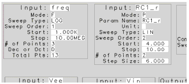
In this example, the value of r:RC1 is set to RC1_r. You must also add a variable called RC1_r to the IC-CAP model variables table and set the variable to a value, such as, 4.000K. In the setup mnsopamp/inv_amp/B_P_macro add an input called RC1_r. The Inputs table is shown in the following figure.
Figure 17 MNS Circuit Parameter Sweep Setup Example
For additional information on sweeping parameters, refer to "Specifying Parameter or Variable Sweeps" in the User's Guide.
The following sections of this chapter describe in more detail each of the steps in these simulation overview examples.