


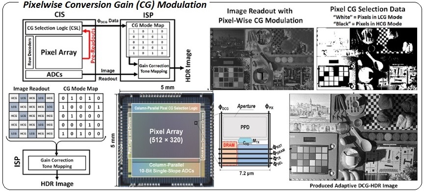
Pixelwise CG/Exposure Modulation for Low-Power Adaptive HDR Imaging
To be updated...

A Smart Camera for Compressive-Sensing based Machine Vision Applications
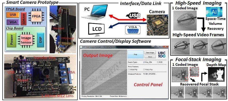
Computational imaging is an emerging field of technology in machine vision, offering digital cameras with unprecedented imaging capabilities. Through exploiting the intrinsic redundancy of scene information, CS-inspired computational cameras overcome the trade-off between spatial resolution and temporal resolution. Several computational camera systems have been developed to demonstrate CS using pixel-wise coded exposure for types of applications such as high-speed imaging, high-dynamic range (HDR) imaging, and depth sensing. However, due to on-chip per-pixel exposure switching is not available in off-the-shelf image sensors, previously reported pixel-wise exposure encoding were realized by programming split-light modulators (SLMs) placed on the camera light path. As SLMs require driving power and accessorial relay lens, they make computational cameras suffer from low light throughput, bulky sizes, and high power consumption. To avoid employing SLMs as the optical modulation apparatus, this research presents a spatial-temporal CS camera system with on-chip coded exposure. Pixel-wise coded exposure is integrated seamlessly into the reset-exposure-readout based operation flow of existing CMOS image sensors. Therefore, CS applications are naturally extended to sensor nodes in a single frame period, which results in a significant reduction in power consumption, simplification of camera module packaging (use common CCM module setups), and minimization of light loss in the optical path. As demonstrations, two CS-based machine vision applications using the proposed computational camera are presented. The CS-based high-speed imaging[J6] can produce high-speed video from a single coded image. By co-operating with lens motors, CS-based focal-stack imaging[J8] is realized to achieve passive depth sening as well as all-in-focus imaging.
CMOS Computational Image Sensor for Pixel-Wise Spatial-Temporal Coded Exposure
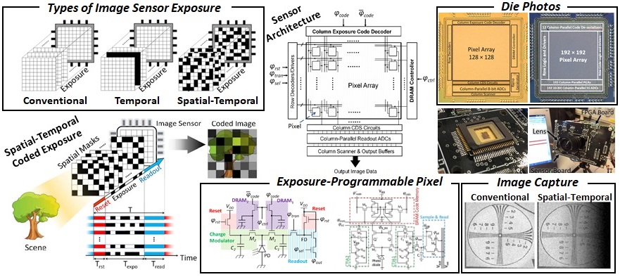
Coded exposure, as a type of Compressive Sensing (CS) technique, employs optical encoding to program the exposure of image sensors. At present, coded exposure has been utilized in computational imaging applications including high dynamic range (HDR) imaging, high-speed imaging, and lens-less imaging. Also, by leveraging CS, computational cameras can acquire depth maps with fewer passive scene measurements. This research explores and focuses on a design of a CMOS image sensor (CIS) capable of coded exposure for CS. Unlike conventional image capture approach which the pixel array of CIS is continuously exposed, Coded exposure, pixels of a coded exposure CIS are intermittently exposed according to either the same sequence (temporal coded exposure) or pixel-wise coded sequence (spatial-temporal coded exposure). To enable on-chip coded exposure, the CIS architecture contains both conventional pixel-signal processing pipelines and novel exposure-code delivery modules. For different types of exposure-programmble pixel (e.g. the APS type in [J6] and the CTIA type in [J8]), corresponding control logics and signal synchronization require fine tuning and precise alignment. By feeding with various types of exposure-code masks, the prototype CIS chips capture images from either non-intermittent exposure (converntional imgaing mode) or intermittent exposure (CS mode). With pixel-wise exposure control capability, coded exposure can also be implemented in Regions of Interest (ROI) with a size down to a single pixel. Such spatial-temporal exposure programming maximizes camera's shutter flexibility and induces CS-based machine vision to sensor plane.
CMOS Exposure-Programmable Pixel
Pixels are the eyes of an image sensor. Along with the fast pace of integrated circuit (IC) fabrication development, pixels are transferred from charge-coupled device (CCD) structures to modern complementary metal-oxide semiconductor (CMOS) designs. Currently, typical CMOS pixel designs such as a 4-transistor (4T) based active-pixel sensor (APS) structure can only perform non-intermittent (non-stop) type of exposure, which prevents CMOS image sensors from many emerging computational imaging applications. In this research, an exposure-programmable CMOS pixel design is proposed. This novel pixel can perform intermittent exposure called “coded exposure”, which has been used in many machine vision applications such as compressive sensing, adaptive high dynamic range (HDR), high-speed motion deblurring, and focal-stack 3D imaging. The proposed pixel consists of a photodetector, selective charge storage units, readout circuitry, and exposure code memory cells. By updating the binary exposure codes stored in the memory cells, charges generated by the photodetector are selectively transferred to designated charge storage units. For example, during the exposure period, when code “1” is in memory, charges are all transferred out from the photodetector to a charge storage unit. If code “0” is stored, charges are transferred to another charge storage unit. At the end, when the exposure is done, only one charge storage unit will be readout for further processing, while other charge storage units are reset to eliminate their stored charges. Therefore, from the pixel output point of view, the pixel has experienced discrete charge integration, which is the target of pixel coded exposure. In circuit implementation, the selective charge storage unit can be realized by either leteral electric-field modulation (LEFM) [C6] or capacitive transimpedance amplifier (CTIA) [J4]. The exposure code memory cells are implemented as either dynamic random-access memory (DRAM) or static random-access memory (SRAM). In verification of such pixel design, a test chip contains 10 × 10 pixels was fabricated in a 0.13µm CMOS process. The pixel is in size of 12.2µm × 12.1µm, using a 2-tap CTIA structure for selective charge storage and 2-bit DRAM cells for exposure codes. Experimental results indicate the pixel array is capable of performing pixel-wise coded exposure in a frame rate of 60fps, with a maximum 5000 binary 10 × 10 exposure code masks applied in each frame.
Smart MEMS Stents for Stenosis Treatment
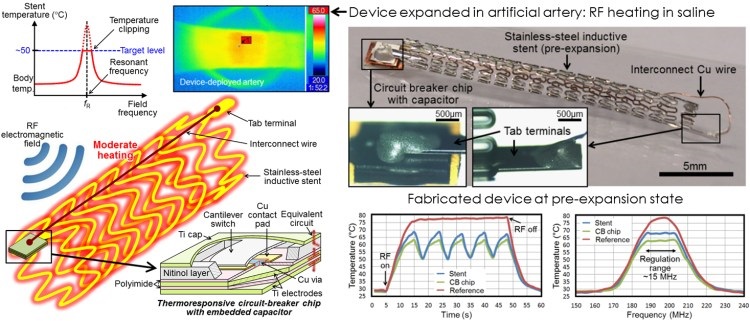
Stents are tubular mechanical devices implanted into arteries to scaffold the channels narrowed by plaque deposition. They are playing vital roles in the treatment of both vascular and non-vascular diseases, with its main application being cardiovascular disease for stenosis management. However, stenting often causes restenosis, i.e., re-narrowing of the vessel. A new class of stent devices, "smart" stents, that are integrated with MEMS transducers to realize advanced diagnosis and treatment of restenosis via implanted stents. One type of them was active stent, RF powered to perform moderate heating of the implanted site toward realizing endohyperthermia treatment of restenosis. A stent-based resonant circuit serves as a frequency-selective wireless heater, applying local thermal stress to the vessel tissue to suppress in-stent restenosis. The biocompatible MEMS circuit breaker chip is integrated with the stent to prevent it from overheating, enabling safeguarded wireless operation of hyperthermia treatment via the implant. This work has demonstrated wireless heating and temperature regulation using fabricated prototypes, which will be further optimized toward their in-vivo studies.
MEMS Circuit Breaker Chip for Biomedical Applications
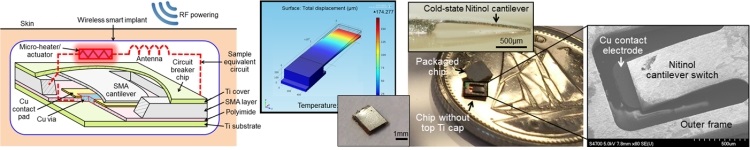
In this work, a novel MEMS circuit breaker was developed for thermal management of biomedical microsystems specifically targeting at implant applications. The circuit breaker was micromachined to have a shape-memory-alloy cantilever actuator as a normally closed temperature-sensitive "smart"' switch to protect the device of interest from overheating, a critical safety feature for intelligent implants with embedded actuators including those that are electrothermally driven. The breaker was microfabricated using biocompatible materials with a chip-based titanium package. The chip is operates in a fully passive manner that removes the need for active sensor and circuitry to achieve temperature regulation in a target device, contributing to the miniaturization of biomedical/implantable microsystems where thermal management is essential.
Quad Beam Piezoresistive Accelerometer
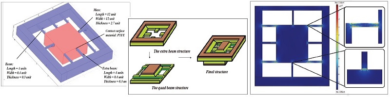
In this work, a new concept of cross-axis sensitivity enhancement for quad beam piezoresistive accelerometers is introduced. By combining a quad-beam structure with extra supporting beams, the cross-axis sensitivity on cross-axis decreases. Instead of using conventional fabrication process, some customized micro-machining processes are proposed for proof-mass shaping and structure combinations. Results show the spring constant increases while the cross-axis sensitivity reduced to ~0.22% of that in primary axis.