Analog Designs
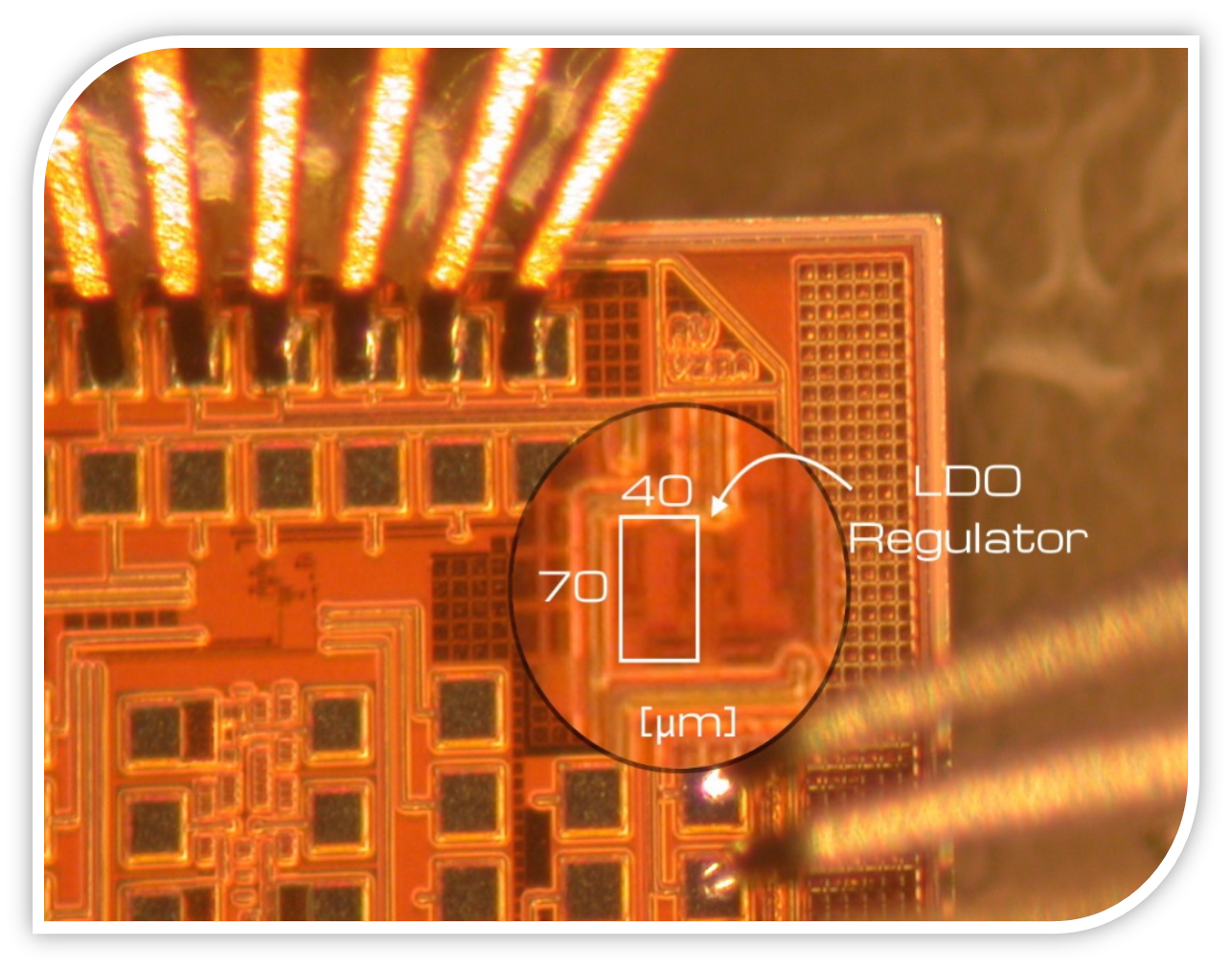
Bulk-Modulated Capacitor-less LDO Regulator
|
An alternative method for improving current delivery and stability of the conventional LDO regulators are investigated. The Measurement results are compared to a conventional LDO regulator with similar characteristics not enhanced by this technique. |
|
|
Process: 0.13 µm CMOS |
|
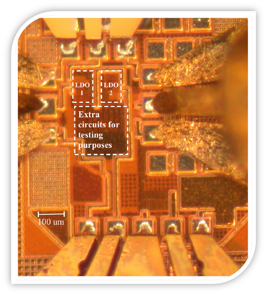
Capacitor-less Ultra Wideband LDO
|
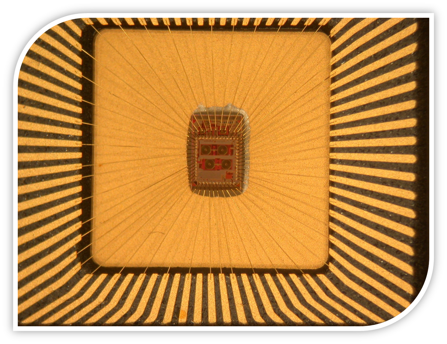
To improve rejection of high frequency ripples as well as speed of load regulations for agile load changes, an ultra-wideband LDO regulator is designed and implemented. This LDO utilizes the reported Compound error amplifier with a different architecture. In the proposed system a novel technique has been proposed to stabilize the system without the use of any off-chip capacitors. |
|
|
Process: 0.13 µm CMOS Area: 4050 µm2 Quiescent Current: 44 µA Load Recovery Time: 160 ns PSR: -21 @ 1 GHz To be published in: IET Journal |
|
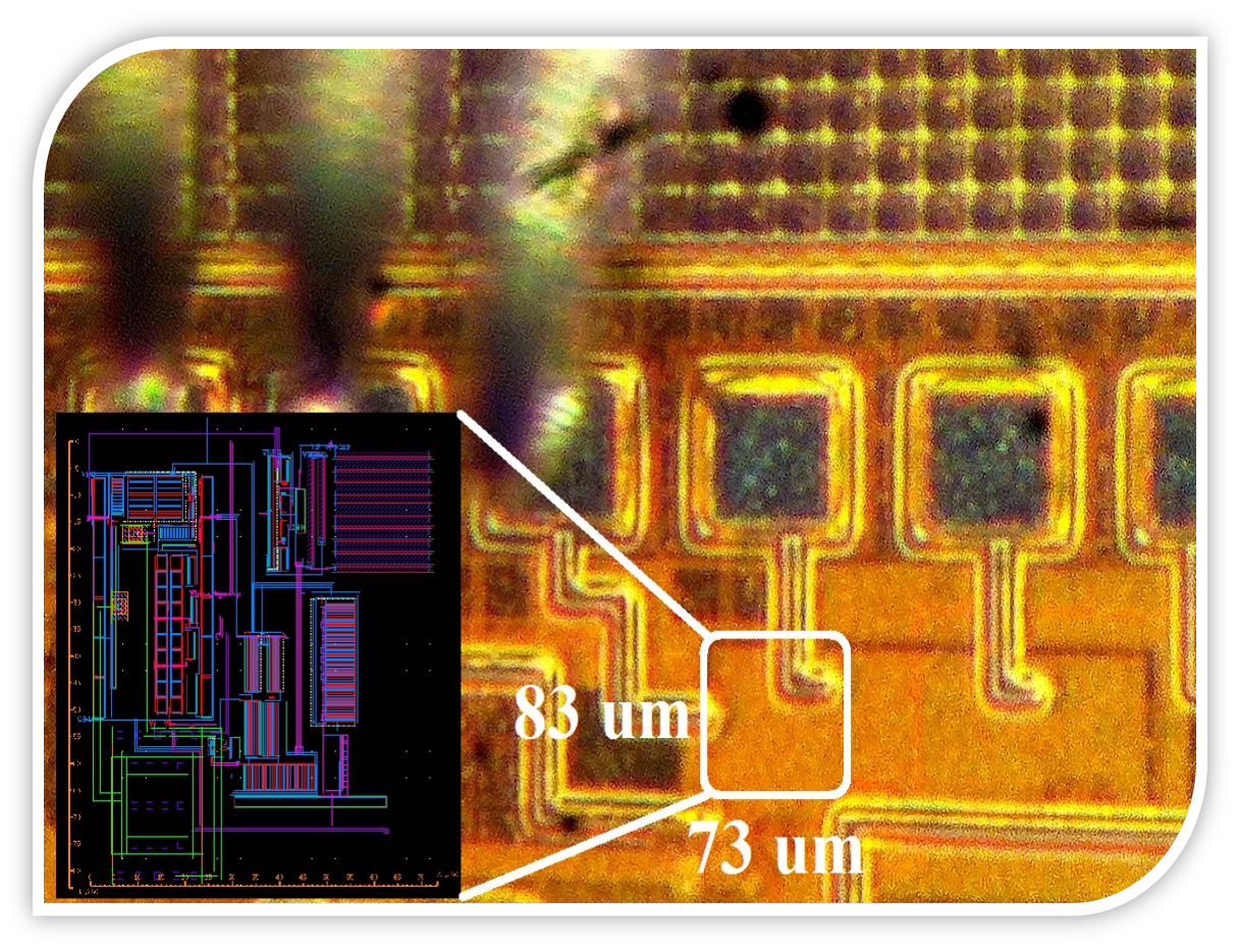
Ultra Wideband Unity Gain Buffer
|
One approach to accurately measure the voltage gain of a high-frequency voltage amplifier which can not derive 50 Ω, is to cascade it with a wideband (or high-band) unity-gain voltage buffer that is capable of driving 50 Ω terminal impedance of RF measurement instruments. On the same note, when it comes to measuring the performance of an integrated VCO, one possible approach can be to use a unity-gain buffer as an interface between measurement instruments and the oscillator under the test. |
|
|
Process: 0.13 µm CMOS |
|
Digital Designs
Phase-Detection Technique for Digital Clock and Data Recovery
|
In an alternative approach for high-speed clock and data recovery that is introduced by one of my colleagues Arash Zargaran Yazd , high speed CML comparator arrays are needed to resolve the high speed input data. For that purpose a CML based digital comparator has been designed and laid out. Below is a brief summary of this design. |
|
|
Process: 90 nm CMOS |
|
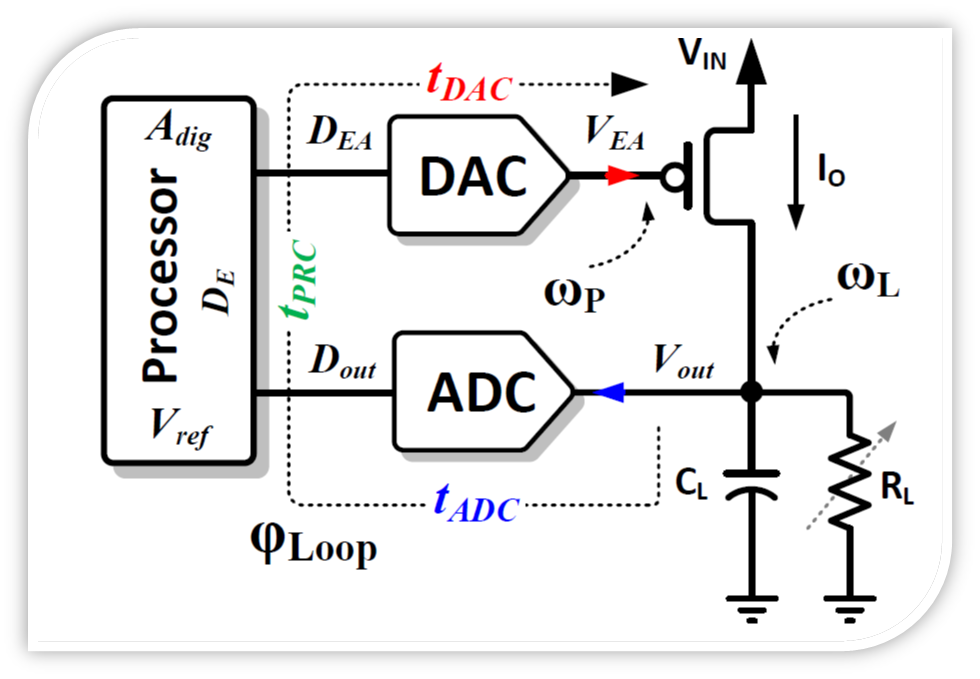
Digitaly Assisted Voltage Regulator
|
In many applications, a DSP unit or microcontroller is utilized to form an ASIC design. This work is showing an approach that can save additional components in such ASIC designs to provide clean supply voltage. This research is using a non-sophisticated microcontroller and one buffer transistor to regulate 2.5V output voltage. The proposed regulator is programmable and studies have been made to ensure its stability under various capacitive and resistive loads. More studies and experimental results are available below. |
|
|
Regulated Output Voltage: 0.1V - 5 V |
|
System-Level Designs
Ultra-Low Power (35 nW) Tele-monitoring System for Bio-medical Applications
|
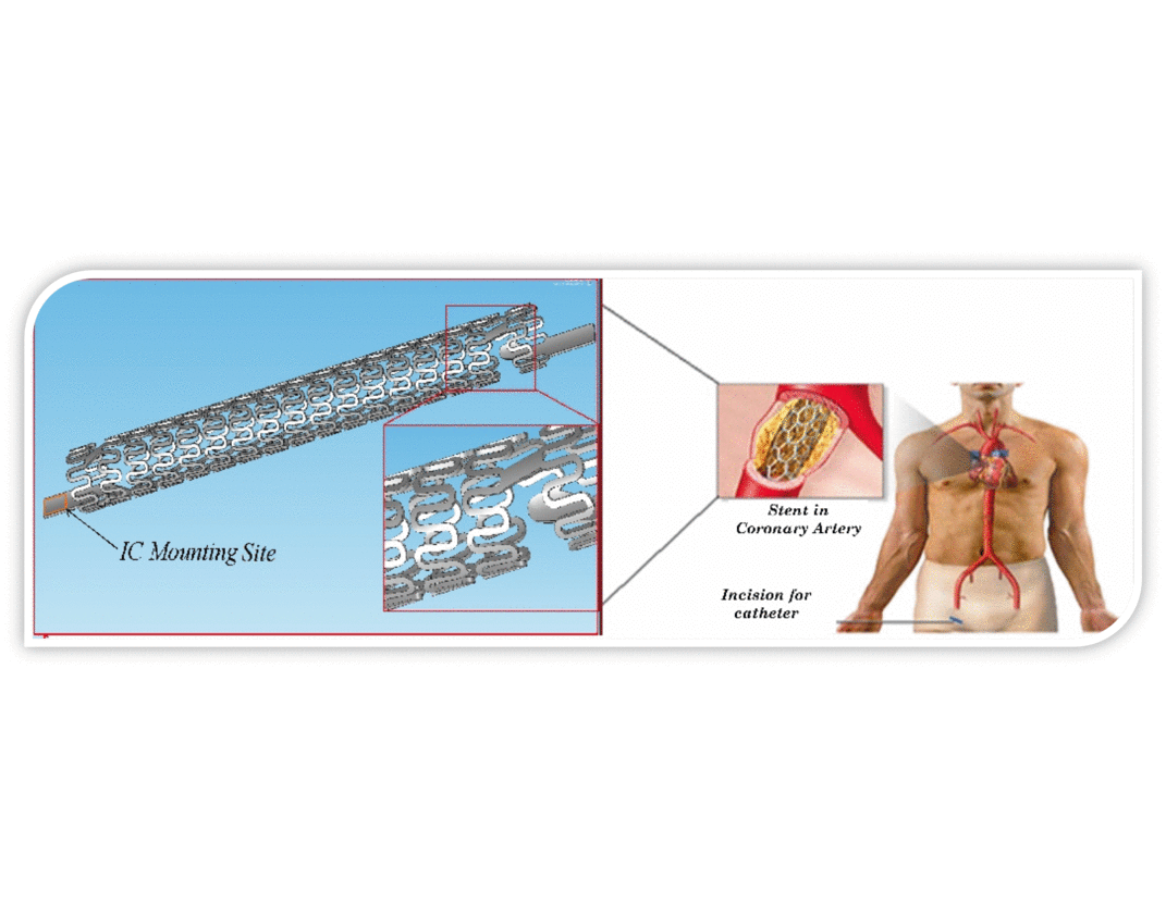
Monitoring the blood pressure at the stented site for patients with angioplasty surgery can give critical information which predicts the potential re-narrowing at the operation site. |
|
|
Process: 0.13 µm CMOS |
|
Low Power, High Resolution Tele-monitoring System for Bio-medical Applications
|
This system is a tele-monitoring system with high-resolution in resolving the pressure changes at the monitoring site. The proof of concept design is customized for monitoring the pressure differences between two sides of the implanted stent at the depth of 5 cm inside a patient's body. The antenna that has been used to power up the system is a modified version of the medical stent which is called Antenna Stent. The Antenna stent (aka Stentenna) has dominant inductive characteristics and can establish an inductive coupling with an external inductive reader. That property can increase the power efficiency and the depth of power delivery. More details on this system is available below. |
|
|
Process: 0.13 µm CMOS |

|
Electromagnetic Analysis and Designs
Study on Wireless Power Transfer to an Implantable Biomedical Device
|
In this work, the optimum frequency of operation for transferring power through live tissues are investigated. Moreover, based on calculated maximum power transfer efficiency and the maximum allowable power density that can be exposed to live tissue (govern by FCC), the maximum deliverable power to a typical implantable biomedical device is obtained. To have an accurate simulation, the biomedical implant (in this work the antenna stent) has been precisely modelled, and the electromagnetic properties of different layers of tissues are carefully gathered and fed into two industrially approved EM simulators, namely Ansys HFSS ™ (High Frequency Structural Simulator) and COMSOL Multiphysics ® |
|
|
Optimum frequency Range: 0.8-1.5 GHz |
|
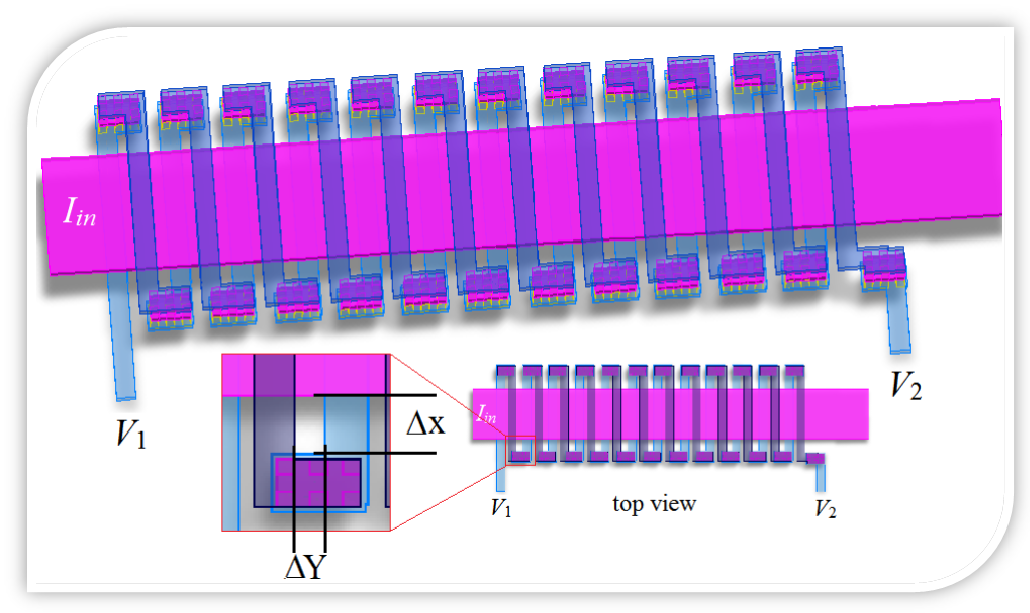
Monolithic Fully Passive High-Frequency Current Sensor Technique
|
In this work, a novel method of sensing the RF current is presented. The proposed technique is fully passive and none-invasive and can be applied into any complex analog and mixed-signal design for fault diagnosis. The current technique requires very little active area and can be adopted in standard CMOS technology. |
|
|
Process: 0.13 μm CMOS |
|
Study on Backscattering Based Tele-monitoring in Biomedical Applications
|
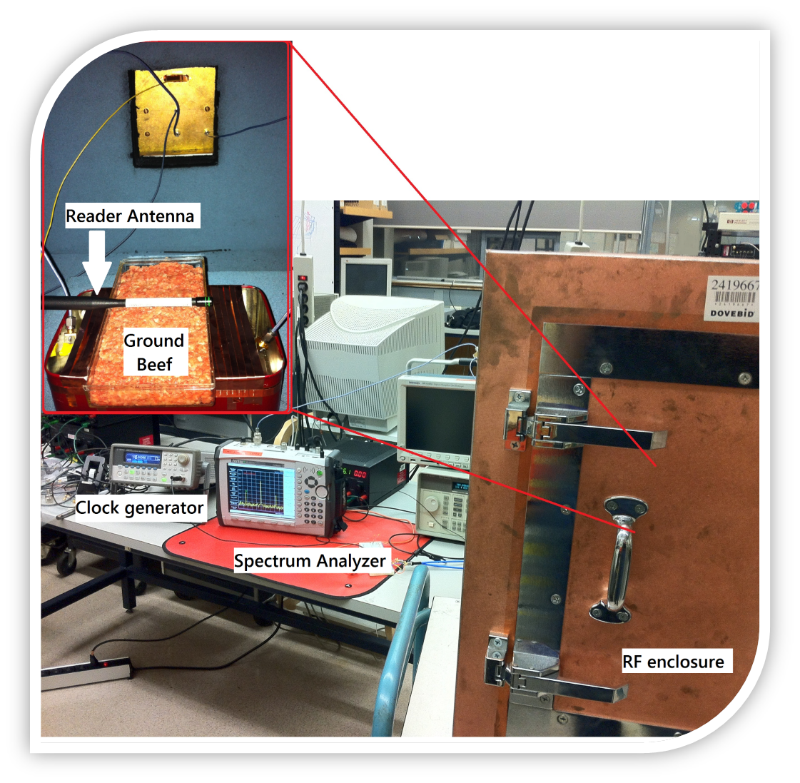
Backscattering technique is a well-known approach in RFID applications. However, when the passive receiver is an implantable biomedical device buried under live tissues, investigations are required to prove its benefits. Backscattering based transmitters (also known as passive oscillators) are significantly less power hungry than "active" oscillators (e.g., VCOs) and therefore there is a great benefit in using them when the power budget is extremely tight. This work uses an antenna stent as an implantable biomedical device and studies the feasibility of this technique in an in-vitro experiment. You can access to full article (it is open-access to public) by clicking on the figure and links below. |
|
|
Dimension of the implantable antenna: 20mmx5mm |
|
Other Activities
iOS App: cheerUP
|
I am finishing up an app for iOS, which I called it CheerUP. You can find some screenshots of the app below. |
|
|
Language: Objective-C |

|
Web Design and CSS: This Website
|
The current website is written with a word editor {Bracket}. There are three main languages involved in the current website. HTML for content, CSS for format and arrangement and Java. As you may have found out already this website rearranges accordingly as you change the window size. The Java is used to add dynamic features to the html and the content. |
|
|
Languages: HTML, CSS, Java scripts (js) |

|
Free Tutorial Videos: Ansoft Maxwell/HFSS
|
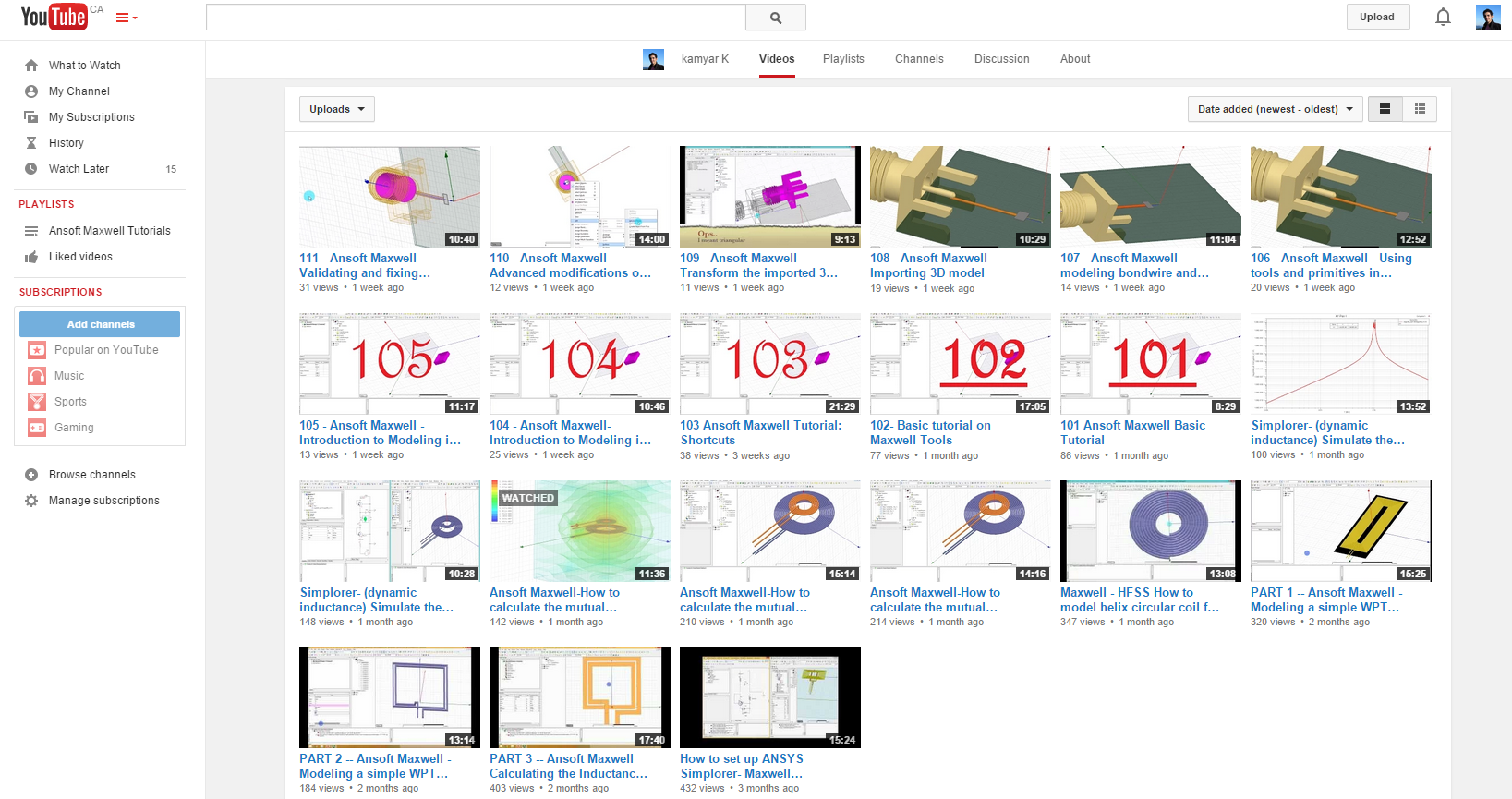
I am trying to share the best of my knowledge with engineers across the globe. One way to do that is through a Youtube Channel. You can follow the link or search for Kamyar K channel. I am currently hosting more than 20 tutorials on my channel and new tutorials are constantly added(as of Jan'15). |
|
|
Languages: English |
|