|
Roberto Rosales
Test Lab Manager
|

|
|
HOME
|
ABOUT ME
|
LAB ACTIVITIES
|
LINKS
|
|
|
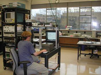
The SoC Test lab is mostly
intended for the test of micro chips designed here at the UBC SoC lab, but is also used for all other kinds of experiments.
Since its opening in 2001 we have tested more than 57 analog, mixed-signal
and digital ICs. The pictures on this page provide examples of activities in
the lab.
|
|
|
|
|
The original setup of the lab for the grand opening in 2001.
The lab today looks the same but with more equipment. In the picture above
Daniel is working on Sameer’s electro Optic
Sampling System.
|
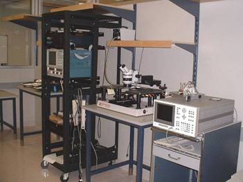
There are two manual probe stations in the lab. A
Cascade RF-1 and a Signatone S-1160 with a hot
chuck. For these we have a collection of probes covering the range from DC to
67GHz.
|
|
|
|
|
The majority of our ICs are manufacture through CMC
scheduled runs. The samples we receive back are either packaged, loose dice,
or loose dice mounted on glass slides.
|
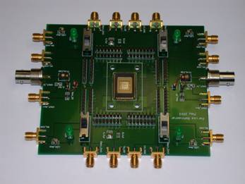
For packaged ICs we frequently design and build our own
test fixtures. The IC on the board is a an interface
circuit for an ultrasonic medical imaging system.
|
|
|
|
|
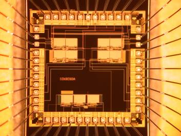
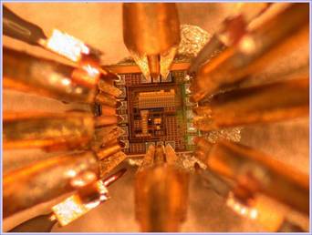
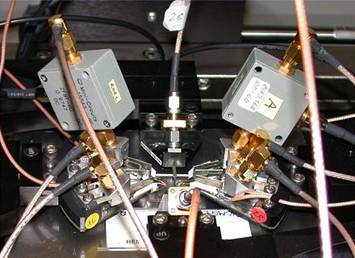
Typical
setup: (Left) setup for a 5GS/s 4bit flash Analog-to-Digital Converter ADC.
(Right) Microphotograph of the IC with the probe tips in contact with the IC
PADS.
|
|
|
|
|
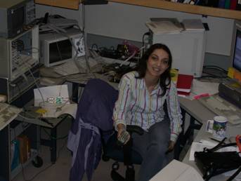
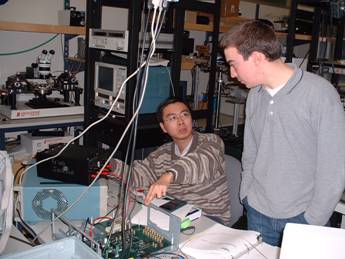
Some students like Shahrzad
(smiling on the left) and Andy (sitting on the right talking to Jim) are
assigned permanent work areas in the test lab. Most other students have their
desks in the cubicle areas of the group in rooms MCLD332 or K4025.
|
|
|
|
|
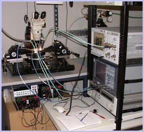
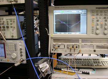
The picture on the left shows the instrumentation used
to test a self-timed interface IC for crossing clock domains. The circuit
under test provides nearly two clock periods of skew tolerance and operates
correctly for any initial phase offset between the transmitter an the
receiver. The picture on the right shows the IC under test on the probe
station.
|
|
|
|
|
The SoC test lab is one of the
main attractions in our department for promotional photo shoots and visits.
On the left is Nima posing with a heat chamber and
his high temperature resisting sensors for pulp and paper. But some times
things get really messy … on the right is Jihong
trapped by the mess in a corner.
|
|
|
|
|
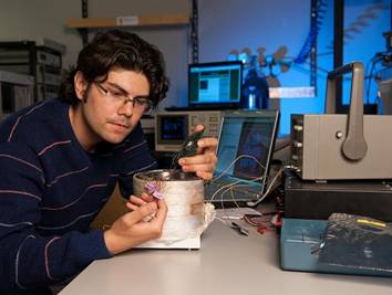
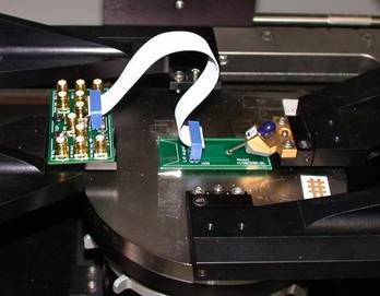
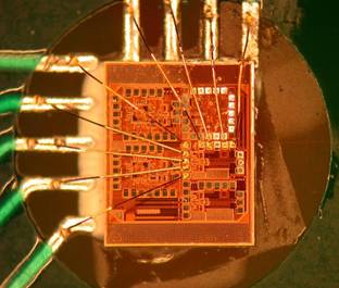
Lately we have been experimenting with die on board as a
test strategy. On the left is a test setup I recently made for Neda’s 60GHz VCO. A loose dice is mounted and wire bonded
directly on a PCB (right) to provide for the DC bias and low frequency
control signals, while the 60GHz output is accessed with a GSG probe.
|
|
|
|
|
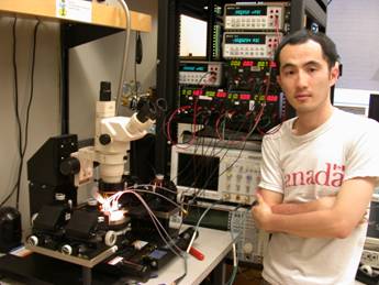
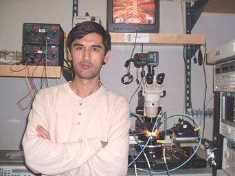
When everything goes well we cannot resist posing for
pictures by the test setup. Above, Michael (left) is testing his on-chip
termination circuit using active inductors and Samad
(right) one of his flash ADC converters.
|
|
Back to Top
|
|
|
|
|
|
|