DISCLAIMER
No, I'm sorry, there's no confidential information in this article! Else I'd have to kill you. But if you would like to find out more, ask me.
Making Chips:
From idea to product, fabless style
Ever wonder how chips are made? What happens in between that idea in somebody's head to that little piece of plastic encased silicon? Well, here's almost all you ever wanted to know! Mostly, this will be based on how PMC-Sierra works, but it will be similar to most other fabless semiconductor companies. (No, let me tell you again, no secret corporate information here)! I won't get in to the technical details, but rather just the general tasks that are required.
Fabless Semiconductor Companies
What's that mean, eh? Well, think you know what a semiconductor company is. Basically, it's synonomous with "chip company". A chip "fab" is short for "fabrication facility" (or factory or whatever). "Fabless" means, well, that you don't have one!
Wait! How can a chip company not make chips? Isn't that silly? Well, not really, sometimes it makes sense to have one, and sometimes it doesn't. If you're really large, like IBM, Intel, Motorola, Texas Instruments or AMD then you definitely want your own fab, especially if you want to work at the cutting edge. But if you're a small company, you have to consider that it takes billions of dollars to build a single fab. To put that into perspective, PMC-Sierra doesn't even make a billion dollars in yearly revenue! Even worse, you have a big expensive fab built up, but sometimes you don't need to use all the capacity, so that's going to waste. Besides which, most "chip" companies core competencies and expertise are in designing electronic circuitry to go on these chips, not how to actually fabricate such devices. Even if you could build one, it's done and then it's obsolete! In the past year, I've seen 3 new process generations for our chips. Each process requires a new fab plant!
So anyways, that's why a lot of new chip companies are fabless. Now everything describe below is fairly common to most fabless companies. Names, titles and duties may differ slightly, but it's a formula that works well, so most people follow it.
In the beginning...
Every device dreamed up requires a team. No engineer ever really works alone, to be a good engineer, you have to be a people person, contrary to what Hollywood might have us believe. (And also, engineers create things, they don't go around fixing them like they do on Star Trek). Because PMC is a relatively small company, most (but not all) departments contributes a single specialist to the project team. And keep in mind, this is not confidential information. Nearly all companies in this space are structured this way. It's just common sense.
Now, I guess I'm gonna sort of separate out the departments, so I can describe it more easily, but keep in mind that almost all departments are involved right from the very beginning.
First up, is Marketing. And it's probably not what you think. The Marketing person is usually a senior engineer, it is not typically an entry level position. Marketing tries to read the market demands, heads out to the customers and, together with senior design engineers, hammers out a specification for a device. So though they are not involved in the technical nitty-gritty, they do have to be knowledgeable about such things. This is only the very beginning, and the project never proceeds past this until funding has been approved.
Creation
Next up are the Design Engineers. Sort of. The bulk of the work will fall to them, so there will usually be more than one engineer on the job. But even in the early stages, the work will have to be done in consultation with Marketing, Validation, Applications and Product Engineering. In Design, there are two types of engineers. The Analog engineers are highly sought after wizards who dabble in black arts. (Well, not really. Every student had to learn the basics, but you gotta love it to do this). Then there are the Digital guys, who are a dime-a-dozen, so to speak. They are basically a bunch of code jockeys. No, it's not the good ol' days anymore. All circuit design is done via programming, using a specialized hardware design language such as "Verilog" or "VHDL". Yes, it's the same as programming in C, Pascal, BASIC or Java. Just a different language. (No, I did not want to be a coder, even though the design guys get more glamour)! They write a lot of code, they test the code, fix the bugs and keep going around until they can't find any more bugs. (Or Marketing comes down and says "Oops! We promised a big customer to have parts tomorrow!"). Once it's done, the data gets handed off the the Layout Engineers, who figure out how to turn their code into polygons. The funny shapes that will be manufactured on silicon. It's not so easy, you can't just put the blocks down and that's it. Sometimes one block is too far away from another one, so there are timing problems with signals. Some layouts are not very efficient in terms of space, so that has to be re-done. There are many little issues to work out here, but eventually after several tries, the layout is complete. Glory time is something called "tape-out", that's when the design is completed and layed out properly.
This here is a very simple layout of a single transistor. Very boring, eh? All those different coloured blocks are each created on a different mask layer.
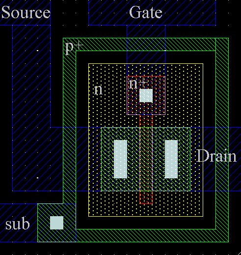
Anyways, it's called "tape-out" because in the old days, the engineers actually used tape to physically mark out the polygon shapes that you see above.
Now the layout data heads to the fabs in Taiwan (where the biggest fab companies in the world are located) via FTP. The data is huge and usually takes overnight to tranfer everything, even at 10 or 100Mbit/s. See? People do use the Internet for real work.
Fab!
What's next? Well, the data has to be turned into something called "masks". Think of masks as film negatives, except in this case, the negatives are chrome on glass. (Also, the masks are build larger than the actual device, and are focused down smaller, opposite with photographic film). Devices are built up in many layers (that's a whole different topic), sort of like doing a trick photo with multiple exposures. Masks sets are very, very expensive. Typical devices nowadays can take 16-25 separate masks and can cost up to half-million dollars per set.
Once completed, the fab (for example, TSMC, the world's largest dedicated fab-only company) takes these masks to make the devices. As I mentioned before, it's just like exposing negatives, except on silicon, not photographic paper. You apply photo-resist, expose with the mask, wash away and repeat with the next mask. (These guys are really good now! They can expose features smaller than the wavelength of light with such techniques as optical-proximity correction and phase-shift masks).
(If you want to learn more, here's a link that has a good summary of what it takes to make a chip: Design of VLSI Systems).
It can take around 6-8 weeks to complete the processing. Now usually, the wafers are tested, then chopped up and packaged. But for the first prototypes, it's a rush job, so the testing part is skipped. The entire wafer is sent straight to a company which specializes in packaging such devices. It chops up the individual devices from the wafer (called "die") and packages every single one of them.
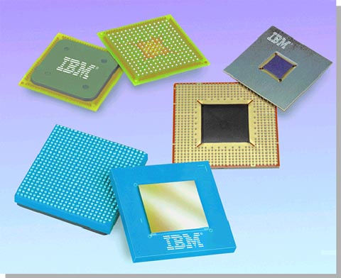
There are all sorts of different package types available, with names like "Quad Flat Package" (QFP), "Dual Inline Package" (DIP) or "Leaded Grid Array" (LGA). However, for high performance devices, nearly everyone has moved to some variation of the "Ball Grid Array" (BGA).
Here's a nice sample of what BGA's look like.
Ready for the Real Thing
Now this is where Product Engineering (that's what I did) comes in! We get to touch silicon (okay, not literally, we're always gloved). We get the first real devices. And this is where there's a little bit of a black art too. You see, when you make a big silicon wafer full of hundreds of devices, inevitably a bunch of them are bad (due to contamination or whatever). The first devices to come back, well, we have to debug test hardware, software and everything else, so it's not easy to figure out if the chip is broken or something else. Psychic powers, that's what it takes to pick out the good devices and hand them off to Validation to test. :)
A Product Engineer makes sure that devices are actually manufacturable. (It's no good being able to do a one-off). That means we have to make sure the design is testable (this comes early on in the design stage), and make changes to the design if it's not. We have to know a little bit about device physics and how fabrication occurs. We have to design the equipment to test and manufacture each device, and write a test program as well. So a little bit of hardware, some software, some of everything. Perfect for someone with a short attention span!
Now for the first night, it is the Validation, (or sometimes called Verification Engineer's, but that is now used for Software Driver Verification) turn to get the glory. After Product Engineering hands them the first devices, Verification usually stays up all night to test the first critical features of the device. Nowadays, they can pretty much send out an e-mail declaring that a device is "alive". (It wasn't always so. Sometimes, you cross your fingers and hope you don't come back with a very expensive resistor. But then Product Engineering can usually tell you that right off the bat).
The Long Road Home...
The Validation Engineer continues working past the first night, of course, and is in charge of testing every single feature of the chip to make sure it functions correctly. And if not, figure out why it doesn't or how to fix it. When you have hundreds of features and endless ways of combining their usage, it's not trivial to figure out if every possible combination works as expected.
At this time, Product Engineering, Validation and Applications are doing the bulk of the work in parallel. Applications will take care of customer issues, including customer support. They will typically need to produce reference designs (for customers to copy :) and answer all sorts of system questions, so they need a high level knowledge of how each device interacts with other devices. They may need to write firmware, BIOS or drivers for the chips. These engineers get very little glory, but are essential.
Very rarely is the first design ever completely correct. It is just too complicated and would take to long to do all the simulations. (Imagine, a normal simulation on just one little sub-block can take 2-3 days on the fastest computers we can buy. On real silicon, the same function can take a couple of milliseconds). Bugs are uncovered and fixes proposed. Testing continues until no more bugs are found (or at least the "deadly" ones anyways). Then, a new revision of the design is taped-out once again. It goes through the same process as before. Hopefully, further revisions on not required...
Once a device revision is considered "good enough", well, here's where Product Engineering gets the glory. Sort of. (Actually, everyone sort of shares in the glory). This is when parts are no longer prototype and are available for general sale. Product Engineering always makes this announcement, since they are the last people to decide whether it's go or no-go. And then afterwards, everyone heads to the pub for beer and wings. (Even if most of us don't drink :)
Acknowledgements
Yes, yes, I'm afraid I was lazy. A lot of these graphics were pilfered from various sites around the WWW. I can take no credit for it. In no particular order, stuff was liberally borrowed from:
IBM
Amkor Technologies.
Related Links
Semiconductor Fabs:
Packaging Houses:
Notes: IBM is a one stop shop, leading edge, but probably more expensive. TSMC is the world's largest fab-only, UMC is 2nd, both based in Taiwan. TSMC will typically service anyone, UMC usually partners with a "customer". Asat is the packaging arm of Chartered (they're related), based in Singapore. Amkor (or Anam) was mainly a Korean concern (but with facilities around the world, including Phillipines), I believe it's the world's largest packaging house.
Take me back to the Library Main Page...