
Design Flow
This section describes the design flow of a digital IC and how the design
flow leads to physical testing. Figure 4 shows the design steps of a digital
IC with the tools supplied by CMC. As the diagram indicates, the first
eight steps are performed in Synopsys and the next three steps are performed
in Cadence.

Figure 4: Design Flow of a Digital IC
The diagram above emphasizes the flow of test vectors which will be
described in the next section. The steps illustrated in the Figure 4 are
as follows:
- VHDL Description
The first step in the design flow is writing the synthesizable register
transfer level (RTL) VHDL circuit model. The VHDL code describes the behaviour
of the circuit.
- Functional Simulation
This part simulates the RTL VHDL model to make sure that it does what it
was designed to do. Functional simulation involves designing a VHDL test
bench that reads stimulus from a file and checks the responses from the
RTL model. The file consists of functional test vectors which can be generated
with a high-level programming language such as C. A vector is the combination
of stimulus and response patterns. In general, the VHDL test bench will
have a clock to synchronize the input of stimulus and the reading of responses
to and from the VHDL model respectively.
- Synthesis
This step compiles the RTL VHDL code from step 1 to a gate level circuit
using a target technology such as BICMOS or CMOS4S. The result is a schematic
diagram of the circuit model that uses the gates provided by the target
technology.
- Scan Insertion
This step adds the scan circuitry to the synthesized circuit for fault
testing purposes.
- Create Test Patterns (ATPG and Scan Check)
This part generates two sets of patterns: Automatic Test Pattern Generation
(ATPG) patterns and Scan Check patterns. The ATPG patterns are used to
test for stuck-at-faults and the scan check patterns are used to test the
scan circuitry to make sure that it is operational. The generated patterns
are in the WGL format. More information on the WGL format is given in the
Synopsys documentation.
- Fault Simulation
Fault simulation uses the patterns generated in the last step as stimulus
to the circuit. This verifies that the scan circuitry and patterns are
correct.
- Gate-Level Simulation
Gate-level simulation verifies that the synthesized circuit with the scan
circuitry works according to functional specifications. The same set of
functional test patterns used in step 2 is used for gate-level simulation.
If the RTL model was synthesized correctly, then the results should be
the same as step 2. Gate-level simulation also verifies that the new scan
circuitry does not affect the functionality of the original circuit. To
perform gate-level simulation, the design is saved as a VHDL file which
uses models from the target technology. Then a test bench that is similar
to the one used for functional simulation is used to input stimulus and
record or compare responses from the design.
- Create EDIF File
After the gate-level circuit has been verified, a EDIF (Electronic Data
Interchange Format) file is created from Synopsys. The EDIF file is a text
representation of the synthesized circuit. This file can be used to import
the design into Cadence to perform the layout steps.
- Place and Route
This part generates the layout of the imported design from Synopsys.
- Gate-Level Simulation (Extracted Netlist)
This part verifies that the layout is functionally correct. Unfortunately,
Cadence only supports Verilog so a test bench written in the Verilog
Hardware Description Language is required. This test bench uses the same
set of functional test patterns as the functional simulation and the first
gate-level simulation.
- Create Stream File and Fabrication
A stream file is created which can be sent to the chip manufacturer for
fabrication.
- Physical Test
Finally, the last step is to test the fabricated chip. For digital ICs,
the HP 75000 Model D20 Test System can be used to perform both functional
and fault testing. As will be described in a later section, the D20 system
has a software tool to import test vectors in the HP PCF (Pattern Capture
Format) format. The next section will describe how PCF files can be generated
from the test patterns shown on the diagram: functional test patterns,
scan check patterns, and ATPG patterns.
Figure 5 describes the steps required to setup the physical testing
of ICs. The CMC tutorial on the physical testing of a digital IC also has
information outlining these steps. The diagram below illustrates the steps
in a slightly different format that contains more information.
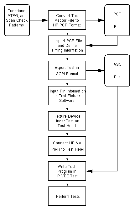
Figure 5: Steps to Setup a Physical Test.
As shown in the diagram, there are eight steps in the physical test
of a digital IC. The rest of the web page deals with these steps in detail.
These steps are briefly described below:
- Convert Test Vector File to HP PCF Format
This step converts functional test vectors in user defined format and WGL
files from Synopsys to HP PCF that can be imported to the D20 Test Development
Software. The next section deals with this topic.
- Import PCF File and Define Timing Information
This step involves designing the physical test with the D20 Test Development
Software. The section HP Test Development Software will discuss this step
in detail.
- Export Test in SCPI Format
In this step, the Test Development Software formulates the test into a
sequence of SCPI commands and saves it to a text file. The text file can
be loaded into the D20 hardware. The text file contains commands to store
test vectors in the memory of each D20 port.
- Input Pin Information in Test Fixture Software
In this step, the pin assignment information is entered into the CMC VXI
Test Head Fixturing Software. The result is several diagrams that illustrate
the jumper connections necessary between the IWA and OWA.
- Fixture Device Under Test on Test Head
This part involves physically connecting the jumpers between the IWA and
OWA. The chip is placed in the PGA socket of the test head and the power
connections are made.
- Connect HP VXI Pods to Test Head
The timing pod and the pattern pods are connected to the test head on the
appropriate sides at this step.
- Write Test Program in HP VEE Test
HP VEE (Visual Engineering Environment) Test is a graphical programming
language for creating test programs. Special device I/O objects are defined
to send SCPI commands to VXI modules and the CMC Test Head (via the serial
port). The HP VEE Test section describes how VEE can be used to perform
the physical testing of ICs.
- Perform Tests
Finally, the tests are performed with the HP VEE Test program from the
previous step.
By now, the reader should have a good understanding of the test equipment
and the design process. Figure 6 summarizes how the components of the test
equipment interact with each other.
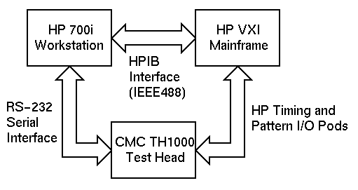
Figure 6: Test Equipment Summary
The next section describes the generation of test vectors for simulation
purposes and physical testing.

