Physics-Based Modeling and Optimization of Power Electronics Converters
In recent years, physics-based system modeling and optimization is gaining more attention. As systems are getting
more complex, it makes more sense to build computer models of the system and to optimize the performance of the system using computer iterations,
rather than manufacturing multiple prototypes and trying to optimize the system through prototypes iterations.
Besides, certain physical phenomena can only be seen through computer models and such visualization gives us insight to further improve the system.
One example of physics_based system modeling in power electronics is to optimize the layout of power converter through Finite Element Analysis (FEA).
Power converters are high-frequency power conversion circuits used to convert a DC or AC input voltage to a DC or AC output voltage having
a larger or smaller magnitude, possibly with opposite polarity or with the isolation of the input and output ground references. LLC Resonant Converter
supplied from a Power Factor Correction (PFC) circuit is a modern topology used in many AC/DC applications such as high-end battery chargers and power supplies.
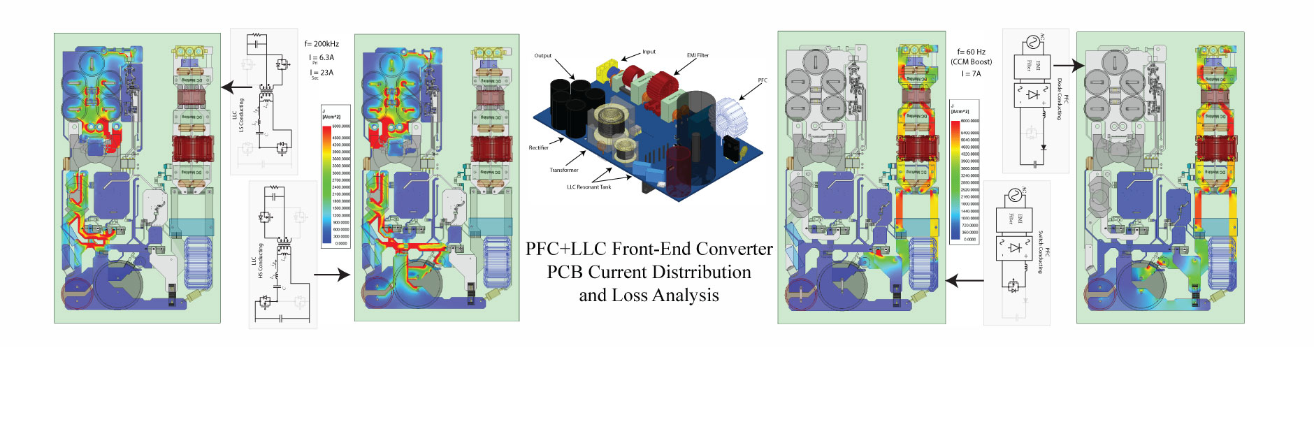
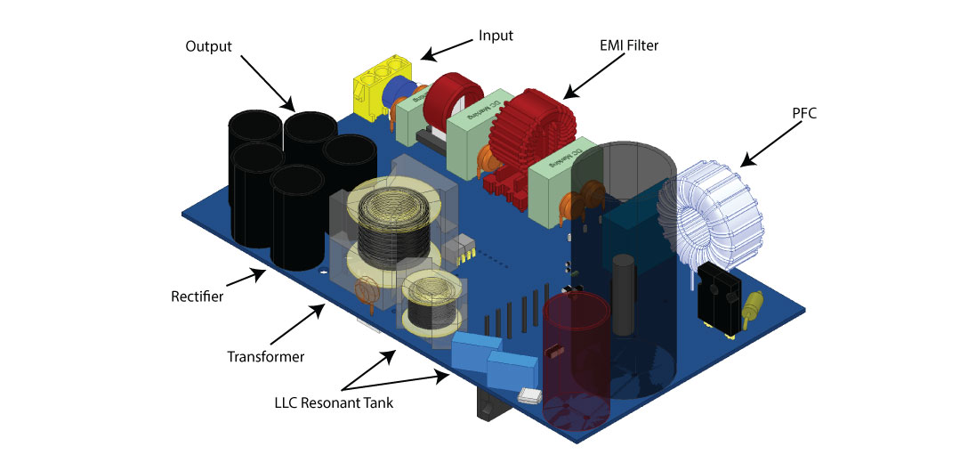
The following figure shows a 1kW PFC+LLC circuit used for 5G applications.
The layput of the converter can be optimized by modeling it through FEA. We can extract the current density distribution in the PCB using ANSYS MAXWELL and find the corresponding PCB losses.
The below figure shows the current density distribution of the LLC converter that operates at 200kHz, at different time intervals. Note the current crowding which happens at the edges of traces as a result of proximity effect.

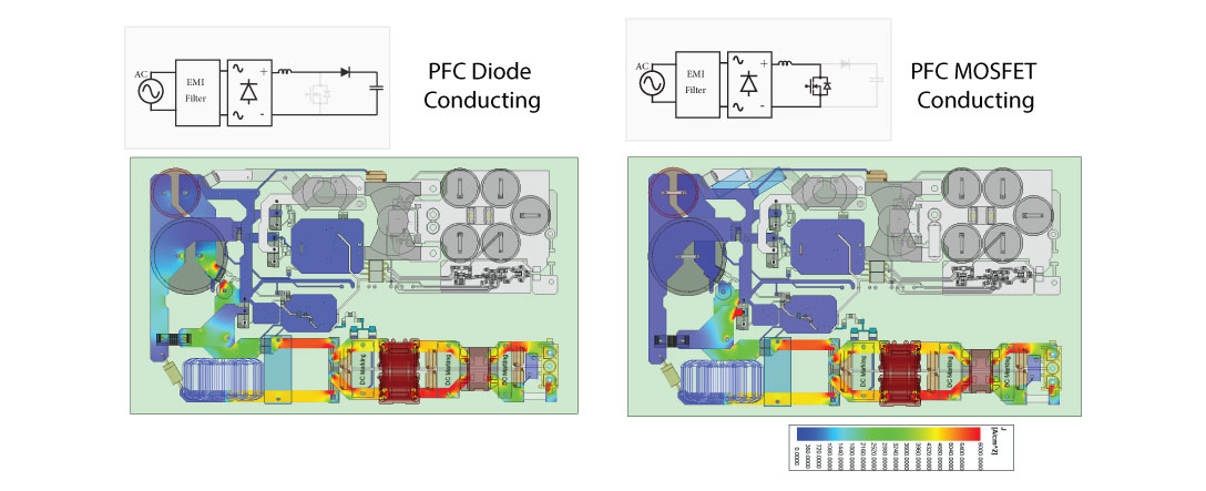
The bellow figure shows the current density distribution of EMI stage and PFC. Since the PFC circuit is a boost converter operating at continious-current-mode (CCM), the major part of the current is low frequency and
so we observe somehow an even current distribution on the traces.
PCB loss extracted using ANSYS MAXWELL then are mapped to ANSYS ICEPAK to extract the temperature distribution. The following figure shows the temperature distribution of the PCB, neglecting other parts of the circuit. This figure shows that
the traces between transformer and the drain of synchronous rectifiers (SR) are the hot spot of the PCB. Please note that in reality these traces have a thermal path to heatsink through MOSFET pins, and so, the temperature of these traces
will be less than what is seen in this figure.

Another application of multi-phsyics modeling in power electronics is to extract the parasitic elements of critical parts of the layout. For instance, the parasitic inductance from gate-driver to gate is a limiting factor in increasing the switching frequency.
With the emerge of gallium nitride (GAN) switches, nowadays switching frequencies in the order of few MHz are reported in both academia and industry. To operate in such high frequencies, it is very important to minimize the parasitic inductance from the gate-driver to the gate.
The following figure shows a trace between the IC driver and the gate. The parasitic elements of this layout can be found using ANSYS Q3D.

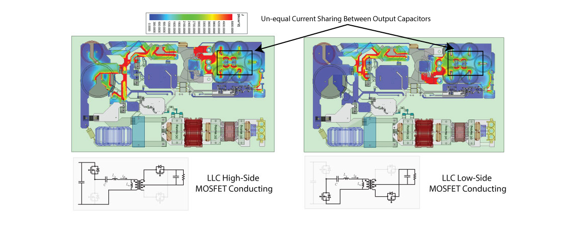
PCB parasitics also come into play for current sharing between parallel components. For instance, the current density distribution on the secondary side of the LLC converter shows that the current is
not equally shared between output capacitors.
Multi-physics modeling also can be used to find the electric field between traces with large voltage differences. Spacing and layout shape is more important in high voltage PCB design rules because a
potential difference between conductive elements on board can create an arc if the voltage between the conductors exceeds the breakdown voltage. FEA also can be used in other areas of power electronics such as modeling and reduction of radiated noise.
Ali Saket
|
26 Feb, 2020
 Expert, ANSYS, MAXWELL, Q3D, SIMPLORER, ICEPAK, SIWAVE, PEXPRT, PEMAG, EMI EMC Engineer, PCB Designer.jpg)