Our first lecture is on Monday, January 9 and our first (official) lab will be on Friday January 13.
The Monday lecture has been moved from 11:30 to 12:30 and the room has been changed from SW1-3170 to SW1-2005.
To accommodate the lecture time change I've updated my office hours to:
all in SW1-3061 (via SW1-3059).
There will be no lab on Friday February 10 or Monday February 13 (Family Day holiday).
I apologize for being very (15 minutes) late to the lecture today. I was in a meeting and didn't notice the alarm. We were going to cover the project guidelines and Verilog sequential statements.
There is only a week left until the deadline for the project proposals. Please review the Project Guidelines to see what you need to do over the next week. Please ask (e-mail or in the discussion forum) if you have any questions and fill out the parts order spreadsheet with the items you need ordered.
The day of the midterm exam date is incorrectly given in the course information handout as Wednesday. February 20 is a Monday.
It has been proposed that we delay the midterm exam until the following week -- to Monday February 27.
You can vote for your preferred date in this survey.
To allow two hours for the exam, it will start during your lunch break (11:30) and continue until the end of our regular lecture (1:30).
Almost all students finish my exams before the time allowed.
Assignment 1 has been posted. It is due February 20.
Since I missed the last lecture, I've changed the due date for the project proposal to midnight Tuesday February 14 to give students a chance to ask questions at the Tuesday lecture.
The midterm exam will be postponed until February 27. There was a sizeable majority (27 to 3) in favor of this change.
The permissions on the the project proposal dropbox were accidentally changed to allow only one submission. If you want to update your submissions feel free to do so (until midnight, February 14).
Because a large-enough classroom is not available for a two-hour slot during on the day of the midterm exam, we will have a two-part midterm exam.
The first part will be on Monday, February 27 and will cover Verilog (declarations, expressions and statements).
The second part on Tuesday, February 28 and will ask you to convert from/to schematics to/from Verilog.
There will be different versions of each midterm and assigned seating (ordering is by surname).
You may use any written/printed materials you wish.
All electronic devices other than a calculator must be turned off and left at the front of the room, in a bag if you wish. This includes cell phones, tablets, notebook computers, media players, headsets, etc.
Lab schedule for the rest of the term:
Feb: 24/27 - Lab 5
March: 3/6, 10/[13], [17]/20, 24/27, 31/3 - Project Work [except Spring Break]
April: 7/10 - Project Demonstrations
Unfortunately, I need to cancel office hours this Thursday (Feb 23) due to an overlapping meeting.
I can be in my office any time on Friday after the lab (8:30 to10:30). Please let me know (by e-mail) if you would like to meet and what time is convenient for you.
You can also ask questions on the (much underutilized) course discussion forum.
All of the ordered parts have arrived. You may pick up your parts and a lab kit during office hours or during a lab.
To connect to the FPGA board you may use the second 40-pin port (JP2) or modify the lab wiring harnesses on JP1 and JP3. If you modify the lab wiring harness you must restore the original configuration before returning the kit so that it can be used in next years' labs. See the DE0 Nano Manual and the ``Lab 0'' handout for the pin assignments.
A limited number of connector housings and wires with pre-crimped pins are available from the instructor.
Before connecting any of the following:
to the FPGA board, please ask me to review your design. Have a schematic and parts layout diagram ready for the review.
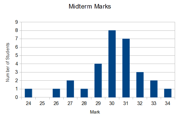
The midterm exams have been marked. The minimum, mean, median, and maximum were 69, 88, 88 and 99% respectively.
The distribution of the marks was:
Unfortunately, I need to cancel office hours this Thursday (March 9) due to an overlapping meeting.
I can be in my office any time on Friday after the lab (8:30 to10:30). Please let me know (by e-mail) if you would like to meet and what time is convenient for you.
You can also ask questions on the (much underutilized) course discussion forum.
The due date for the final project report is currently April 7 (the date of the first project demos).
It can be changed to a later date if desired. I have set up a survey with a few additional choices.
You can vote for your preferred dates before midnight on Monday, April 3.
I have enabled anonymous postings on the course discussion forum. Other students will not be able to tell who posted a question (but the instructor will).
The results of the vote to change the due date are:
|
Thursday April 13 (last day of classes) |
||||
|
Monday April 17 (last day before exams) |
There were 9 votes. I have changed the due date to April 17.
You may, of course, submit your report earlier than the due date.
Your submission will be considered incomplete unless you include the completed LIB-73 "Creative Commons BY-NC-ND" license allowing your report to be made public (see the course information handout for more information).
Some suggestions for you project -- and other -- presentations:
The course information document says you will need to submit:
"A final report fully documenting what was achieved. It should include block diagrams, schematics, code listings, photos, etc.)"
In response to a question about report length on the discussion forum I added:
Take a look at the reports submitted for the project courses at other Universities/Institutes.
- It would be nice if you explained the motivation behind the project.
- Your report should briefly summarize what your project does and how it works so the reader doesn't have to look at your design documents to figure it out.
- The bulk of the report should be enough technical detail (block diagrams, state machine diagrams, schematics, Verilog code, program listings, photos, plans, 3D images, etc.) so another student can (easily) understand and reproduce your project.
Somewhere on the order of 10 to 30 pages should be sufficient to describe your project. [But feel free to make your report longer or shorter if necessary.]
Remember that your report will be published. Review the guidelines in the course information handout regarding including personal information in the report (e.g. don't include your BCIT ID number).
Based on questions asked during the demonstrations I would also add:
To sign the library release form (lib_73.pdf) you have a various choices. These include:
I will be in my office (SW1-3061) on:
I can answer questions, collect project FPGA boards and components, and scan release forms (if necessary).
Although this is not a complete list, you should be prepared to answer the following types of questions for the final exam:
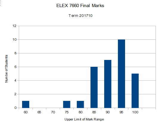
The final marks for the course have been computed and posted under Content/Course Information/marks and the marking scheme to Content/Course Information/Marking Scheme. The final exam and solutions have been posted to Content/Exams. Comments about the project have been posted to the feedback section of the project report dropbox. The distribution of the final marks is shown below. Please let me know if you have any questions.